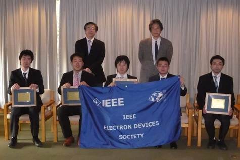
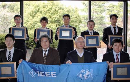
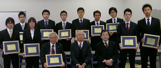
Awards
IEEE EDS Japan Joint Chapter Student Award
IEEE EDS Japan Joint Chapter have established "Japan Chapter Student Award" in 2002 to encourage student researchers to participate academic societies and stimulate their research activities.
This is awarded to young researchers from a university or graduate school in Japan who has made a significant contribution to electronic device technology. Award winners will be selected from student researchers who have made oral presentations as the first author at important international conferences sponsored by IEEE EDS. The chapter officers or judges appointed by the chapter will check the status of presentations at target conferences, and we will not accept self- or other-nominations for this award.
This award is eligible for student members of IEEE EDS or those who have completed the membership application process by the time that the award is presented. Please check About Us to join the student membership.
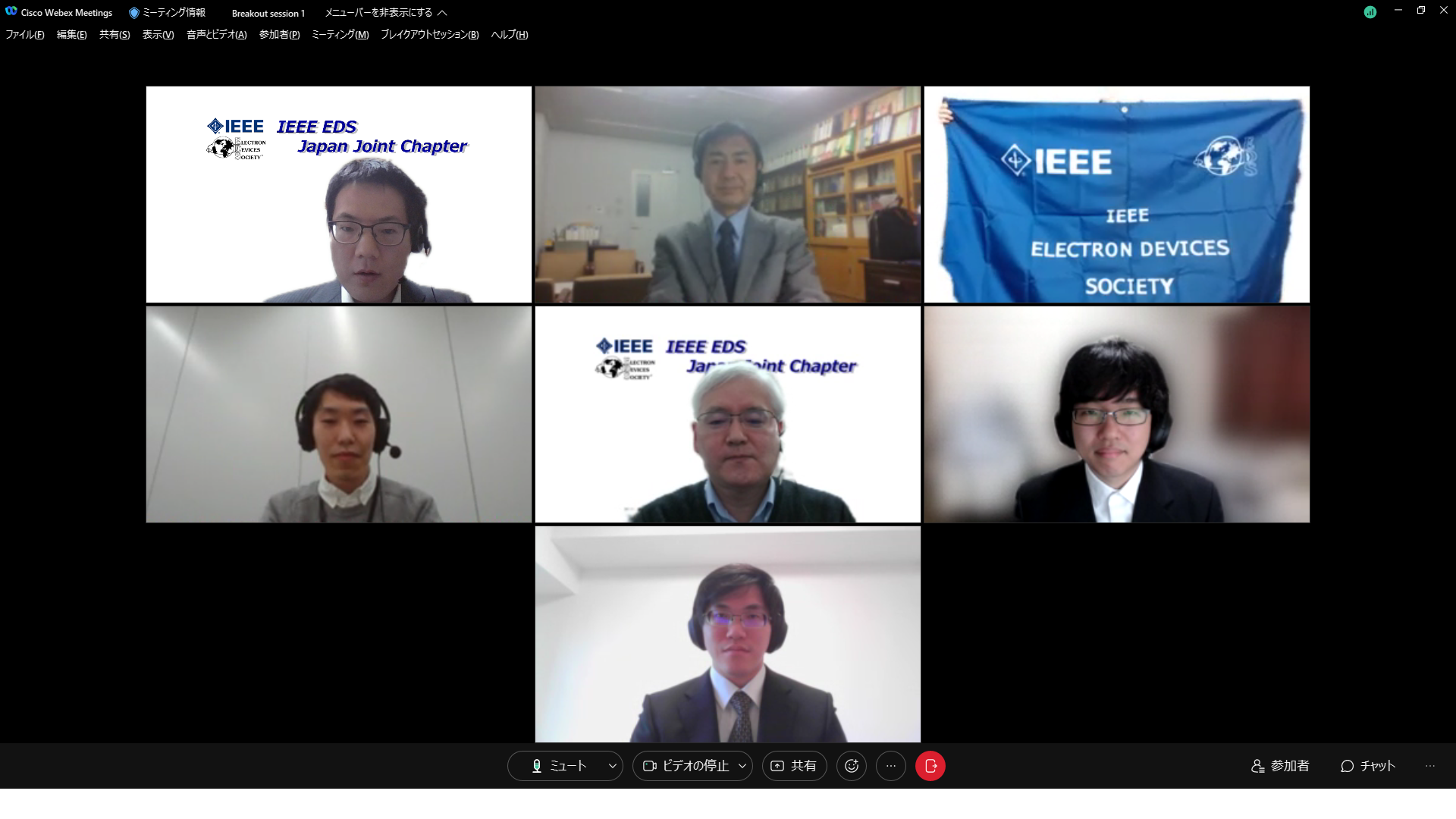
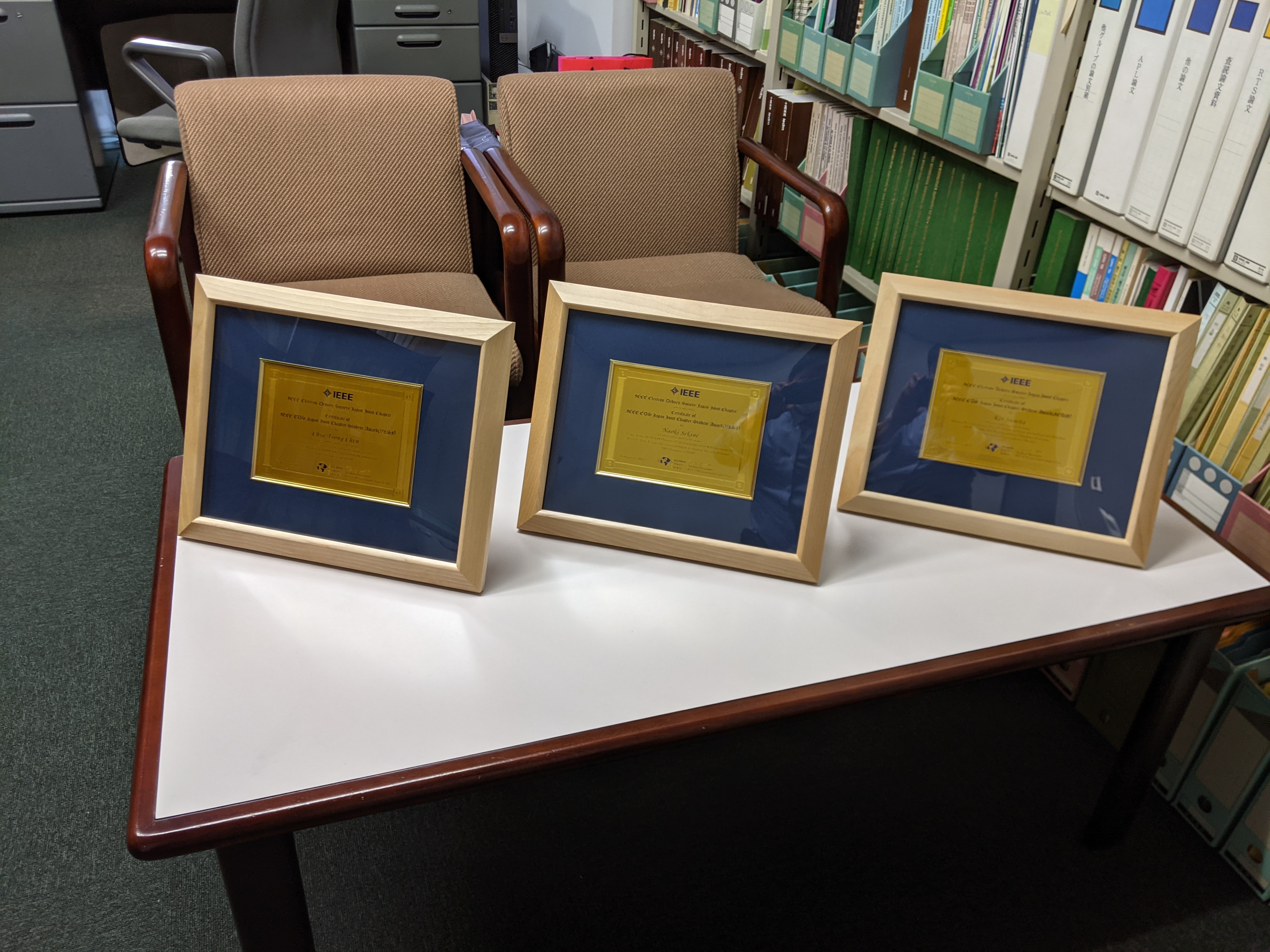
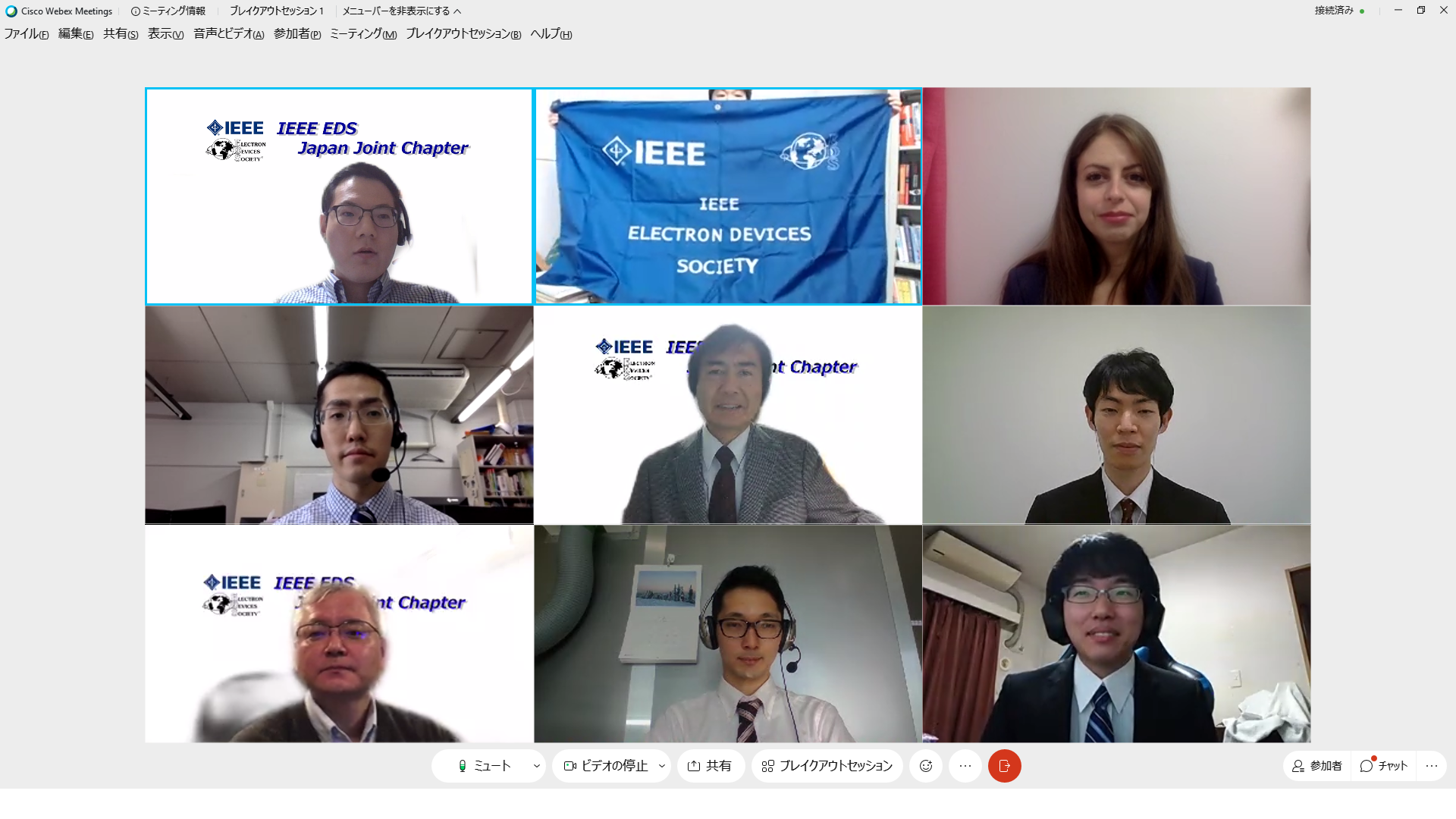
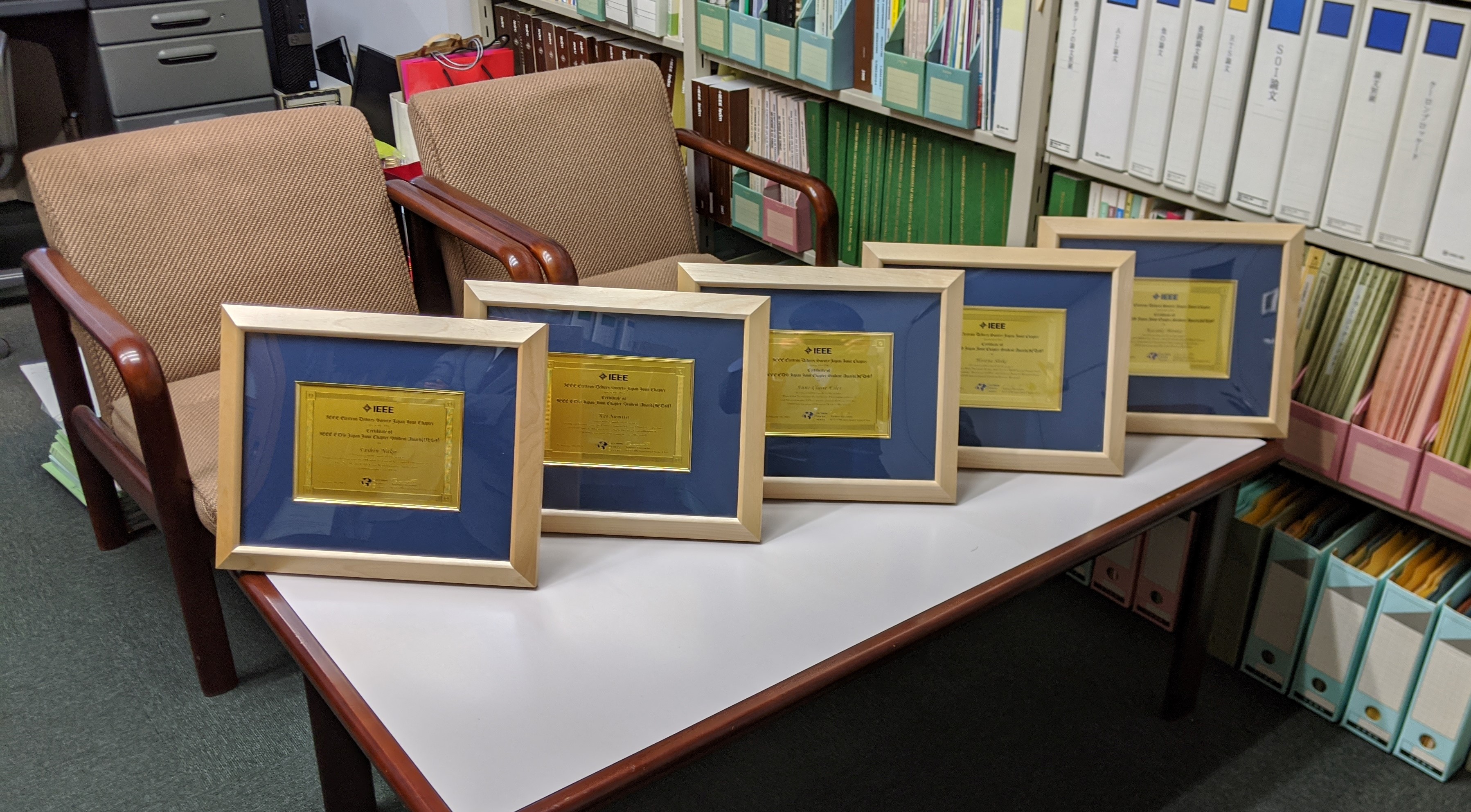
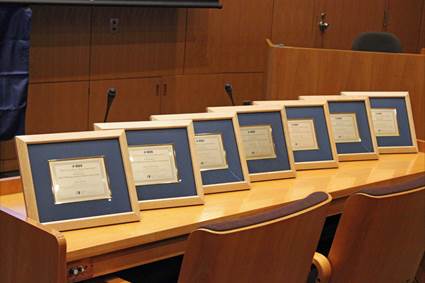
Award ceremony will be held on February every year and a certificate plaque will be awarded to the winners.
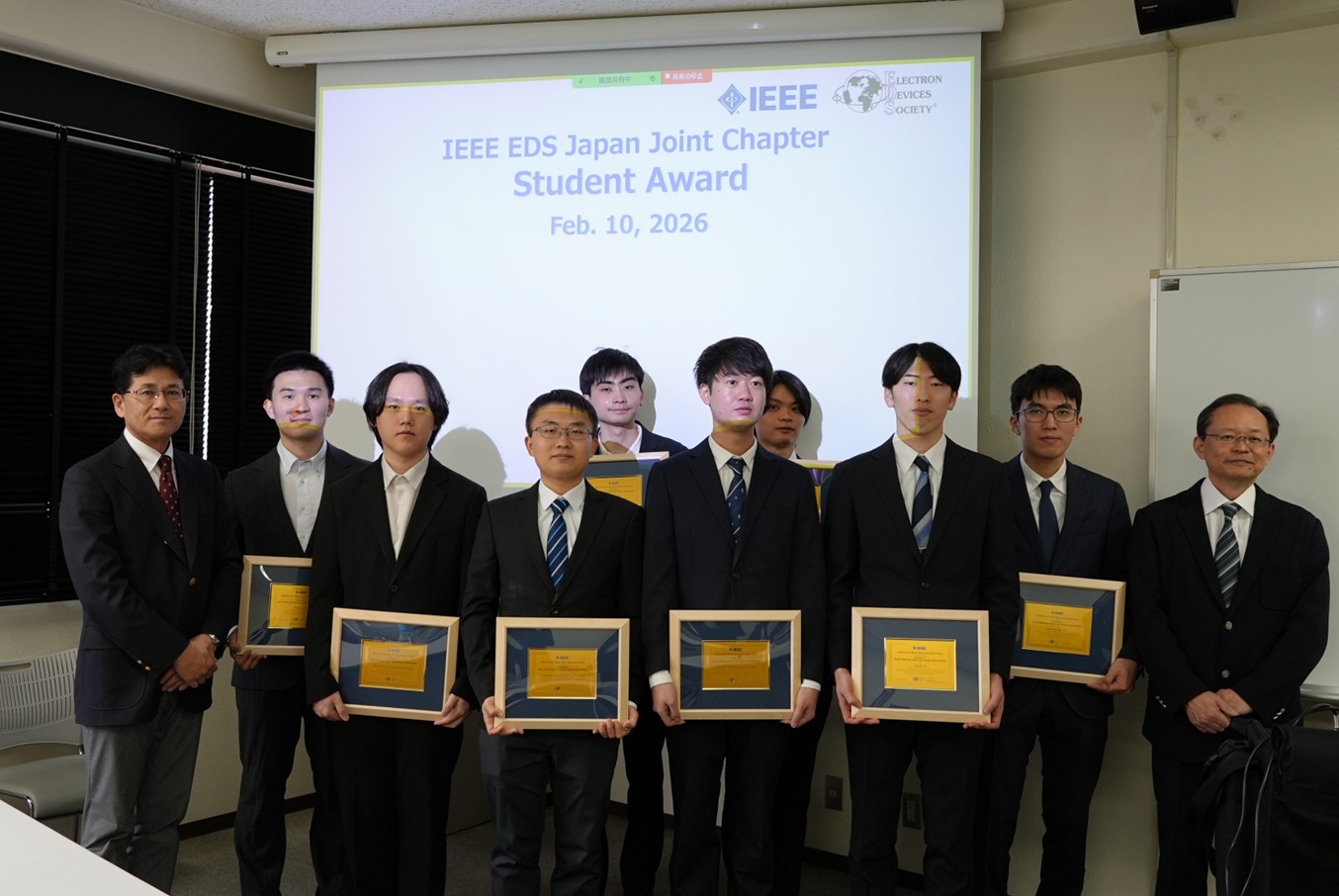
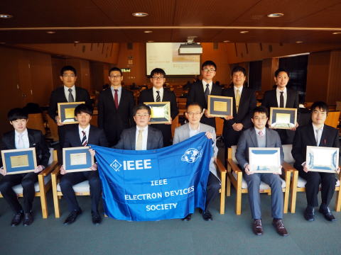
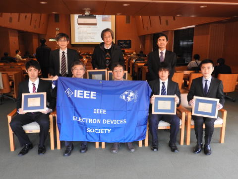
24th 2025 IEEE EDS Student Award ()
IEEE EDS Japan Chapter Student Award (VLSI)
- Anlan Chen, Ki-woong Park, Kota Sakai, The University of Tokyo
"A Gate-All-Around Nanosheet Oxide Semiconductor Transistor by Selective Crystallization of InGaOx for Performance and Reliability Enhancement" - Ritaro Takenaka, The University of Tokyo
"A 76.5-dB Dynamic-Range 8-bit 100-MS/s Variable-Range SAR ADC" and
"An 11.9-ENOB 560-MS/s Subranging ADC Employing Amplifier-Switching Architecture with Multi-Threshold Comparators" - Kosuke Ito, The University of Tokyo
"Revealing wake-up mechanism in ultra-thin ferroelectric HZO: Domain de-pinning triggered by oxygen vacancy annihilation exhibiting optimal wake-up frequency"
IEEE EDS Japan Chapter Student Award (IEDM)
- Xingyu Huan, The University of Tokyo
"On the Statistical Variability of High-Performance Crystalline InGaOx Nanosheet Oxide Semiconductor FETs" - Kohei Takizawa, Tohoku University
"A 120 dB Dynamic Range 3D Stacked 2-Stage LOFIC CMOS Image Sensor with Illuminance-Adaptive Signal Selection Function" - Tomohiro Akazawa, The University of Tokyo
"Ultralow-power, High-speed Integrated Si Photonic Switch Enabled by III-V/Si Hybrid MOS Optical Phase Shifters"
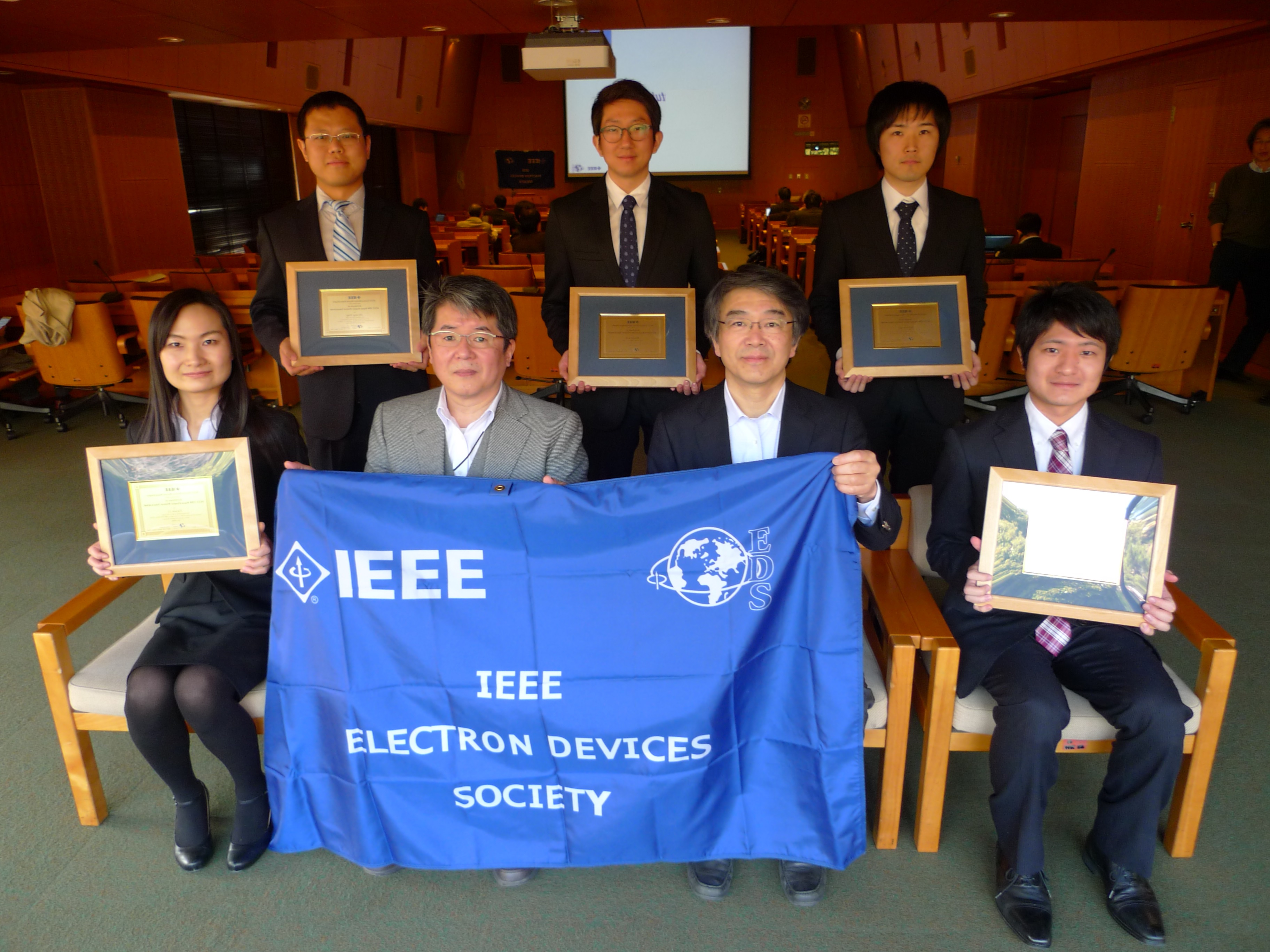
23rd 2024 IEEE EDS Student Award ()
IEEE EDS Japan Chapter Student Award (VLSI)
- Kaito Hikake, Sung-hun Kim, Xingyu Huang, The University of Tokyo
"Scaling Potential of Nanosheet Oxide Semiconductor FETs for Monolithic 3D Integration-ALD Material Engineering, High-Field Transport, Statistical Variability" - Yi Zhang, Institute of Science Tokyo
"A 28GHz 4-Stream Time-Division MIMO Phased-Array Receiver Utilizing Nyquist-Rate Fast Beam Switching for 5G and Beyond" - Hiroaki Kitaike, Kyoto University
"A 0.9-2.6pW 0.1-0.25V 22nm 2-bit Supply-to-Digital Converter Using Always-Activated Supply-Controlled Oscillator and Supply-Dependent Activation Buffers for Bio-Fuel-Cell-Powered-and-Sensed Time-Stamped Bio-Recording" - Masaki Otomo, The University of Tokyo
"Revealing Mechanism of Non-accumulative Disturb and Approach Toward Disturb Suppression in HZO/Si FeFET Memory" - Chenxin Liu, Institute of Science Tokyo
"A 640-Gb/s 4×4-MIMO D-Band CMOS Transceiver Chipset" - Sena Kato, Institute of Science Tokyo
"A 28GHz 5G NR Wirelessly Powered Relay Transceiver Using Rectifier-Type 4th-Order Sub-Harmonic Mixer"
IEEE EDS Japan Chapter Student Award (IEDM)
- Seong-kun Cho, The University of Tokyo
"Unveiling memory-window narrowing mechanism after bipolar cycling in HZO/Si FeFETs: Critical role of hole trap generation and carrier de-trapping behavior" - Xilun Chi, Kyoto University
"Unique electron trapping and its impacts on electron mobility in SiC n-channel MOSFETs"
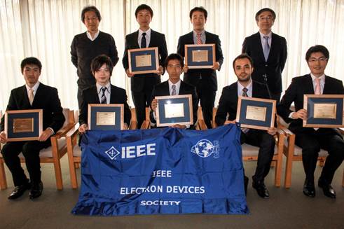
22nd 2023 IEEE EDS Student Award()
IEEE EDS Japan Chapter Student Award (VLSI)
- Chun Wang, Tokyo Institute of Technology
"A Sub-THz Full-Duplex Phased-Array Transceiver with Self-Interference Cancellation and LO Feedthrough Suppression" - Junnosuke Suzuki, Tokyo Institute of Technology
"Pianissimo: A Sub-mW Class DNN Accelerator with Progressive Bit-by-Bit Datapath Architecture for Adaptive Inference at Edge" - Zuocheng Cai, The University of Tokyo
"HZO Scaling and Fatigue Recovery in FeFET with Low Voltage Operation: Evidence of Transition from Interface Degradation to Ferroelectric Fatigue" - Kaito Hikake, The University of Tokyo
"A Nanosheet Oxide Semiconductor FET Using ALD InGaOx Channel and InSnOx Electrode with Normally-Off Operation, High Mobility and Reliability for 3D Integrated Devices"
IEEE EDS Japan Chapter Student Award (IEDM)
- Takeru Kumabe, Nagoya University
"Demonstration of AlN-based Vertical p-n Diodes with Dopant-Free Distributed-Polarization Doping"
21st 2022 IEEE EDS Student Award()
IEEE EDS Japan Chapter Student Award (VLSI)
- Chia-Chi Kuo, Tohoku University
"A 4-Tap CMOS Time-of-Flight Image Sensor with In-pixel Analog Memory Array Achieving 10Kfps High-Speed Range Imaging and Depth Precision Enhancement" - Eishin Nako, The University of Tokyo
"Experimental demonstration of novel scheme of HZO/Si FeFET reservoir computing with parallel data processing for speech recognition" - Tomohiro Akazawa, The University of Tokyo
"Low-capacitance Ultrathin InGaAs Membrane Photodetector on Si Slot Waveguide towards Receiver-less System"
IEEE EDS Japan Chapter Student Award (IEDM)
- Yuto Miyatake, The University of Tokyo
"Record-low Loss Non-volatile Mid-infrared PCM Optical Phase Shifter based on Ge2Sb2Te3S2"
20th 2021 IEEE EDS Student Award()
IEEE EDS Japan Chapter Student Award (VLSI)
- Chia Tsong Chen, The University of Tokyo
"Impact of Asymmetric Strain on Performance of Extremely-Thin Body (100) GOI and (110) SGOI pMOSFETs" - Naoki Sekine, The University of Tokyo
"Bandgap-Tunable III-V-OI Photonics Platform with Quantum Well Intermixing for Versatile Active-Passive Integration of Chip-Scale Photonic Integrated Circuits"
IEEE EDS Japan Chapter Student Award (IEDM)
- Kei Sumita, The University of Tokyo
"Optimum Design of Channel Material and Surface Orientation for Extremely-Thin-Body nMOSFETs under New Modeling of Surface Roughness Scattering"
19th 2020 IEEE EDS Student Award()
IEEE EDS Japan Chapter Student Award (VLSI)
- Eishin Nako, The University of Tokyo
"Proposal and Experimental Demonstration of Reservoir Computing using Hf0.5Zr0.5O2/Si FeFETs for Neuromorphic Applications"
IEEE EDS Japan Chapter Student Award (IEDM)
- Kei Sumita, The University of Tokyo
"Subband Engineering by Combination of Channel Thickness Scaling and (111) Surface Orientation in InAs-On-Insulator nMOSFETs" - Anne-Claire Eiler, The University of Tokyo
"Thin-Film Transistor Platform for Electrophysiological and Electrochemical Characterization of Biological Cells" - Hiroya Shike, Tohoku University
"A Global Shutter Wide Dynamic Range Soft X-ray CMOS Image Sensor with BSI Pinned Photodiode, Two-stage LOFIC and Voltage Domain Memory Bank" - Kazuki Monta, Kobe University
"Secure 3D CMOS Chip Stacks with Backside Buried Metal Power Delivery Networks for Distributed Decoupling Capacitance"
18th 2019 IEEE EDS Student Award()
IEEE EDS Japan Chapter Student Award (VLSI)
- Masaki Abe, Chuo University
"Pre-shipment Data-retention/Read-disturb Lifetime Prediction & Aftermarket Cell Error Detection & Correction by Neural Network for 3D-TLC NAND Flash Memory" - Chengji Jin, The University of Tokyo
"Transient Negative Capacitance as Cause of Reverse Drain-induced Barrier Lowering and Negative Differential Resistance in Ferroelectric FETs" - Tsung-En Lee, The University of Tokyo
"Improvement of SiGe MOS interface properties with a wide range of Ge contents by using TiN/Y2O3 gate stacks with TMA passivation" - Fei Mo, The University of Tokyo
"Experimental Demonstration of Ferroelectric HfO2 FET with Ultrathin-body IGZO for High-Density and Low-Power Memory Application"
IEEE EDS Japan Chapter Student Award (IEDM)
- Kanako Ando, Kagawa University
"Highly Sensitive Silicon Slip Sensing Imager for Forceps Grippers Used under Low Friction Condition" - Takuya Maeda, Kyoto University
"Impact Ionization Coefficients in GaN Measured by Above- and Sub-Eg Illuminations for p-/n+ Junction"
17th 2018 IEEE EDS Student Award()
IEEE EDS Japan Chapter Student Award (VLSI)
- Yusuke Yamaga, Chuo University
"5x Reliability Enhanced 40nm TaOx Approximate-ReRAM with Domain-Specific Computing for Real-time Image Recognition of IoT Edge Devices" - Kwang-Won Jo, The University of Tokyo
"Hole mobility enhancement in extremely-thin-body strained GOI and SGOI pMOSFETs by improved Ge condensation method"
IEEE EDS Japan Chapter Student Award (IEDM)
- Maasa Murata, Tohoku University
"A 24.3Me- Full Well Capacity CMOS Image Sensor with Lateral Overflow Integration Trench Capacitor for High Precision Near Infrared Absorption Imaging" - Fei Mo, The University of Tokyo
"Scalability Study on Ferroelectric-HfO2 Tunnel Junction Memory Based on Non-equilibrium Green Function Method with Self-consistent Potential" - Masahiro Yamamoto, Tohoku University
"A CMOS Proximity Capacitance Image Sensor with 16um Pixel Pitch, 0.1aF Detection Accuracy and 60 Frames Per Second" - Takuya Maeda, Kyoto University
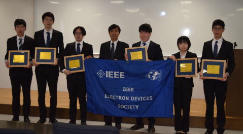
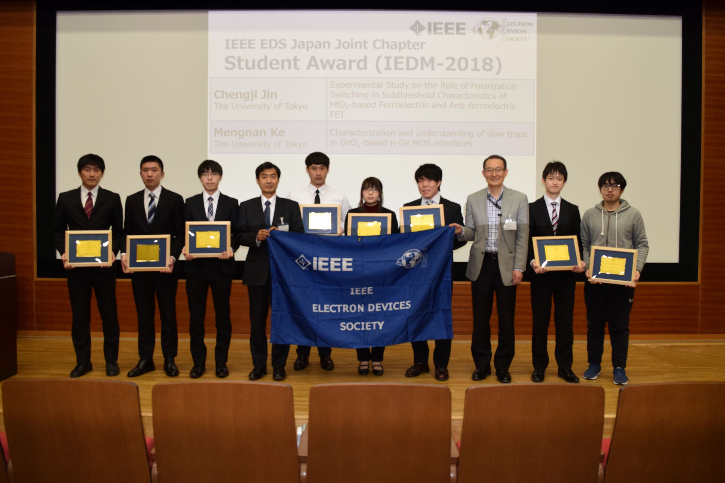
"Parallel-Plane Breakdown Fields of 2.8-3.5 MV/cm in GaN-on-GaN p-n Junction Diodes with Double-Side-Depleted Shallow Bevel Termination" - Chengji Jin, The University of Tokyo
"Experimental Study on the Role of Polarization Switching in Subthreshold Characteristics of HfO2-based Ferroelectric and Anti-ferroelectric FET" - Mengnan Ke, The University of Tokyo
"Characterization and understanding of slow traps in GeOx-based n-Ge MOS interfaces"
16th 2017 IEEE EDS Student Award()
IEEE EDS Japan Chapter Student Award (VLSI)
- Hiroshi Oka, Osaka University
"Enhancement-mode n-channel TFT and Room-temperature Near-infrared Emission Based on n+/p junction in Single-crystalline GeSn on Transparent Substrate" - Masashi Haraguchi, Keio University
"A 6Gb/s Rotatable Non-Contact Connector withHigh-Speed/I2C/CAN/SPI Interface Bridge IC" - Wu-Kang Kim, The University of Tokyo
"High Performance 4.5-nm-Thick Compressively-Strained Ge-on-Insulator pMOSFETs Fabricated by Ge Condensation with Optimized Temperature Control" - Yoshiaki Deguchi, Chuo University
"Flash Reliability Boost Huffman Coding (FRBH): Co-Optimization of Data Compressionand VTH Distribution Modulation to Enhance Data-Retention Time by over 2900x"
IEEE EDS Japan Chapter Student Award (IEDM)
- Kyoji Mizoguchi, Chuo University
"Lateral Charge Migration Suppression of 3D-NAND Flash by Vth Nearing for Near Data Computing" - Xuan Tian, The University of Tokyo
"Sub-nm EOT Ferroelectric HfO2 on p+Ge with Highly Reliable Field Cycling Properties"
15th 2016 IEEE EDS Student Award()
IEEE EDS Japan Chapter Student Award (VLSI)
- Dae-Hwan Ahn (The University of Tokyo)
"Performance improvement of InxGa1‐xAs Tunnel FETs with Quantum Well and EOT scaling" - Atsuro Kobayashii (Chuo University)
"Versatile TLC NAND Flash Memory Control to Reduce Read Disturb Errors by 85% and Extend Read Cycles by 6.7‐times of Read‐Hot and Cold Data for Cloud Data Centers" - Hidetake Sugo (Tohoku University)
"A Dead-time Free Global Shutter CMOS Image Sensor with in-pixel LOFIC and ADC using Pixel-wise Connections" - Sho Ikeda (Tokyo Institute of Technology)
"An 8.865‐GHz ‐244dB‐FOM High‐Frequency Piezoelectric Resonator‐Based Cascaded Fractional‐N PLL with Sub‐ppb‐Order Channel Adjusting Technique"
IEEE EDS Japan Chapter Student Award (IEDM)
- Manabu Suzuki (Tohoku University)
"An Over 1Mfps Global Shutter CMOS Image Sensor with 480 Frame Storage Using Vertical Analog Memory Integration" - Junjie An (University of Tsukuba)
"Experimental Demonstration of -730V Vertical SiC p-MOSFET with High Short Circuit Withstand Capability for Complementary Inverter Applications" - Chih-Yu Changi (The University of Tokyo)
"Impact of La2O3/InGaAs MOS Interface on InGaAs MOSFET Performance and its Application to InGaAs Negative Capacitance FET" - Hiroshi Oka (Osaka University)
"High-mobility TFT and Enhanced Luminescence Utilizing Nucleation-controlled GeSn Growth on Transparent substrate for Monolithic Optoelectronic Integration" - Lun Xu (The University of Tokyo)
"General Relationship for Cation and Anion Doping Effects on Ferroelectric HfO2 Formation" - Jae-Hoon Han (The University of Tokyo)
"Extremely High Modulation Efficiency III-V/Si hybrid MOS Optical Modulator Fabricated by Direct Wafer Bonding"
14th 2015 IEEE EDS Student Award()
IEEE EDS Japan Chapter Student Award (VLSI)
- Cimang Lu (東京大学)
"Design and Demonstration of Reliability-aware Ge Gate Stacks with 0.5 nm EOT" - Koichi Nishi (東京大学)
"High Hole Mobility Front-gate InAs/InGaSb-OI Single Structure CMOS on Si" - Hao Qiu (東京大学)
"Impact of Random Telegraph Noise on Write Stability in Silicon-on-Thin-BOX (SOTB) SRAM Cells at Low Supply Voltage in Sub-0.4V Regime" - Senju Yamazaki(中央大学)
"Reliability Enhancement of 1X nm TLC for Cold Flash and Millennium Memories"
IEEE EDS Japan Chapter Student Award (IEDM)
- Xiao Yu (東京大学)
"Experimental Study on Carrier Transport Properties in Extremely-Thin Body Ge-on-Insulator (GOI) p-MOSFETs with GOI Thickness Down to 2 nm" - Xiuyan Li (東京大学)
"Self-decomposition of SiO2 due to Si-chemical Potential Increase in SiO2 between HfO2 and Substrate - Comprehensive Understanding of SiO2-IL Scavenging in HfO2 Gate Stacks on Si, SiGe and SiC -" - Shoichi Kabuyanagi (東京大学)
"Effects of Free-carriers on Rigid Band and Bond Descriptions in Germanium - Key to Designing and Modeling in Ge Nano-devices -"
13th 2014 IEEE EDS Student Award()
IEEE EDS Japan Chapter Student Award (VLSI)
- Sheyang Ning (東京大学、中央大学)
"23% Faster Program and 40% Energy Reduction of Carbon Nanotube Non-volatile Memory with Over 1011 Endurance" - Sang Hyeon Kim (東京大学)
"High Performance InGaAs-On-Insulator MOSFETs on Si by Novel Direct Wafer Bonding Technology applicable to Large Wafer Size Si" - Akitsugu Ueda (東京大学)
"Ultra-Low Voltage (0.1V) Operation of Vth Self-Adjusting MOSFET and SRAM Cell"
IEEE EDS Japan Chapter Student Award (IEDM)
- Xiuyan Li (東京大学)
"Analytical Formulation of SiO2-IL Scavenging in HfO2/SiO2/Si Gate Stacks:A Key is the SiO2/Si Interface Reaction" - Minsoo Kim (東京大学)
"High Ion/Ioff Ge-source Ultrathin Body Strained-SOI Tunnel FETs - Impact of Channel Strain, MOS Interfaces and Back Gate on the Electrical Properties" - Akito Suzuki (早稲田大学)
"Source-induced RDF Overwhelms RTN in Nanowire Transistor: Statistical Analysis with Full Device EMC/MD Simulation Accelerated by GPU Computing"
12th 2013 IEEE EDS Student Award()
IEEE EDS Japan Chapter Student Award (VLSI)
- Choong Hyun Lee (東京大学)
"Enhancement of High-Ns Electron Mobility in Sub-nm EOT Ge n-MOSFETs" - Sang Hyeon Kim (東京大学)
"Strained Extremely-Thin Body In0.53Ga0.47As-On-Insulator MOSFET on Si Substrates" and
"High Performance Extremely-Thin Body InAs-On-Insulator MOSFETs on Si with Ni-InGaAs Metal S/D by Contact Resistance Reduction Technology"
IEEE EDS Japan Chapter Student Award (IEDM)
- Dariush Hassan Zadeh (東京工業大学)
"Low Dit High-k/In0.53Ga0.47As Gate Stack, with CET Down to 0.73 nm and Thermally Stable Silicide Contact by Suppression of Interfacial Reaction" - Go Oike (東京大学)
"High Electron Mobility (>16 cm2/Vsec) FETs with High On/Off Ratio (>106) and Highly Conductive Films (σ>102 S/cm) by Chemical Doping in Very Thin (~20 nm) TiO2 Films on Thermally Grown SiO2" - Muneki Akazawa (広島大学)
"Local Transfer of Single-Crystalline Silicon (100) Layer by Meniscus Force and Its Application to High-Performance MOSFET Fabrication on Glass Substrate" - Shunsuke Koba (神戸大学)
"The Impact of Increased Deformation Potential at MOS Interface on Quasi-Ballistic Transport in Ultrathin Channel MOSFETs Scaled down to Sub-10 nm Channel Length" - Munetaka Noguchi (東京大学)
"High Ion/Ioff and Low Subthreshold Slope Planar-Type InGaAs Tunnel FETs with Zn-Diffused Source Junctions"
11th 2012 IEEE EDS Student Award()
IEEE EDS Japan Chapter Student Award (VLSI)
- Rui Zhang (東京大学)
"High Mobility Ge pMOSFETs with 0.7 nm Ultrathin EOT using HfO2/Al2O3/GeOx/Ge Gate Stacks Fabricated by Plasma Post Oxidation" - Sang Hyeon Kim (東京大学)
"Sub-60 nm Deeply-Scaled Channel Length Extremely-thin Body InxGa1-xAs-On-Insulator MOSFETs on a Si with Ni-InGaAs Metal S/D and MOS Interface Buffer Engineering"
IEEE EDS Japan Chapter Student Award (IEDM)
- Kentaro Kukita (大阪大学)
"Impact of Quasi-Ballistic Phonon Transport on Thermal Properties in Nanoscale Devices: A Monte Carlo Approach" - Takashi Matsumoto (京都大学)
"Impact of Random Telegraph Noise on CMOS Logic Delay Uncertainty under Low Voltage Operation" - Nobuyasu Beppu (東京工業大学)
"Experimental Study of Self-Heating Effect (SHE) in SOI MOSFETs: Accurate Understanding of Temperatures During AC Conductance Measurement, Proposals of 2ω Method and Modified Pulsed IV"
10th 2011 IEEE EDS Student Award()
IEEE EDS Japan Chapter Student Award (VLSI)
- Rui Zhang (東京大学)
"High Mobility Ge pMOSFETs with ~1nm Thin EOT Using Al2O3/GeOx/Ge Gate Stacks Fabricated by Plasma Post Oxidation" - Sang Hyeon Kim (東京大学)
"High Performance Extremely-Thin Body III-V-On-Insulator MOSFETs on a Si Substrate with Ni-InGaAs Metal S/D and MOS Interface Buffer Engineering" - Yasuhiro Nakajima (東京大学)
"Phase Transformation Kinetics of HfO2 Polymorphs in Ultra-Thin Region"
IEEE EDS Japan Chapter Student Award (IEDM)
- Yoshiharu Yonai (東京工業大学)
"High drain current (>2A/mm) InGaAs channel MOSFET at VD=0.5V with shrinkage of channel length by InP" - Teruyuki Ohashi (東京工業大学)
"Experimental Evidence of Increased Deformation Potential at MOS Interface and Its Impact on Characteristics of ETSOI FETs" - Tsunaki Takahashi (東京工業大学)
"Thermal-Aware Device Design of Nanoscale Bulk/SOI FinFETs: Suppression of Operation Temperature and Its Variability" - Tomoyuki Yokota (東京大学)
"Sheet-type Organic Active Matrix Amplifier System using Vth-Tunable, Pseudo-CMOS Circuits with Floating-gate Structure"
Past award winners
2010年 第9回
- Naotoshi Kadotani 角谷 直哉 (東京工業大学)
"Anomalous Electron Mobility in Extremely-Thin SOI (ETSOI) Diffusion Layers with SOI Thickness of Less Than 10 nm and High Doping Concentration of Greater Than 1x1018cm-3" (2010 IEDM) - Sang Hyeon Kim 金 相賢 (東京大学)
"Self-aligned Metal Source/Drain InxGa1-xAs n-MOSFETs Using Ni-InGaAs Alloy" (2010 IEDM) - Choong Hyun Lee 李 忠賢 (東京大学)
"Ge MOSFETs Performance: Impact of Ge Interface Passivation" (2010 IEDM) - Xiaowei Song 宋 驍嵬 (東京大学)
"Impact of DIBL Variability on SRAM Static Noise Margin Analyzed by DMA SRAM TEG" (2010 IEDM) - Makoto Suzuki 鈴木 誠 (東京大学)
"Direct Measurements, Analysis, and Post-Fabrication Improvement of Noise Margins in SRAM Cells Utilizing DMA SRAM TEG" (2010 Symp. on VLSI Technology) - Kiichi Tachi 舘 喜一 (東京工業大学)
"Experimental Study on Carrier Transport Limiting Phenomena in 10 nm Width Nanowire CMOS Transistors" (2010 IEDM) - Keita Yamaguchi 山口 慶太 (筑波大学)
"Universal Guiding Principle for the Fabrication of Highly Scalable MONOS-Type Memories -Atomistic Recipes Based on Designing Interface Oxygen Chemical Potential-" (2010 IEDM)
2009年 第8回
- Miyuki Kouda 幸田 みゆき (東京工業大学)
"Charged Defects Reduction in Gate Insulator with Multivalent Materials" (2009 Symp. on VLSI Technology) - Ken Shimizu 清水 健 (東京大学)
"Physical Understandings of Si (110) Hole Mobility in Ultra-Thin Body pFETs by <110> and <111> Uniaxial Compressive Strain" (2009 IEDM) - Makoto Suzuki 鈴木 誠 (東京大学)
"Post-Fabrication Self-Convergence Scheme for Suppressing Variability in SRAM Cells and Logic Transistors" (2009 Symp. on VLSI Technology) - Tsunaki Takahashi 高橋 綱己 (東京工業大学)
"Direct Observation of Subband Structures in (110) pMOSFETs under High Magnetic Field: Impact of Energy Split Between Bands and Effective Masses on Hole Mobility" (2009 IEDM) - Kiichi Tachi 舘 喜一 (東京工業大学)
"Relationship Between Mobility and High-k Interface Properties in Advanced Si and SiGe Nanowires" (2009 IEDM) - Shuhei Tanakamaru 田中丸 周平 (東京大学)
"A 0.5V Operation, 32% Lower Active Power, 42% Lower Leakage Current, Ferroelectric 6T-SRAM with VTH Self-Adjusting Function for 60% Larger Static Noise Margin" (2009 IEDM) - Jiezhi Chen 陳 杰智 (東京大学)
"High Hole Mobility in Multiple Silicon Nanowire Gate-All-Around pMOSFETs on (110) SOI" (2009 Symp. on VLSI Technology) - Kohei Nakanishi 中西 洸平 (筑波大学)
"Self-Consistent Monte Carlo Device Simulations Under Nano-Scale Device Structures: Role of Coulomb Interaction, Degeneracy, and Boundary Condition" (2009 IEDM) - Arifin Tamsir Putra (東京大学)
"A New Methodology for Evaluating VT Variability Considering Dopant Depth Profile" (2009 Symp. on VLSI Technology) - Kiyohito Morii 森井 清仁 (東京大学)
"High Performance GeO?/Ge nMOSFETs with Source/Drain Junctions Formed by Gas Phase Doping" (2009 IEDM) - Keita Yamaguchi 山口 慶太 (筑波大学)
"Atomistic Guiding Principles for MONOS-Type Memories with High Program/Erase Cycle Endurance" (2009 IEDM) - Choong Hyun Lee 李 忠賢 (東京大学)
"Record-high Electron Mobility in Ge n-MOSFETs Exceeding Si Universality" (2009 IEDM)
2008年 第7回
- Yusaku Kato 加藤 祐作 (東京大学)
"A Large-Area, Flexible, Ultrasonic Imaging System With A Printed Organic Transistor Active Matrix" (2008 IEDM) - Shoma Kuga 久我 翔馬 (早稲田大学)
"Precise Detection Of Single Mismatched DNA With Functionalized Diamond Electrolyte Solution Gate FET" (2008 IEDM) - Ken Shimizu 清水 健 (東京大学)
"Experimental Investigation on the Origin of Direction Dependence of Si(110) Hole Mobility Utilizing Ultra-Thin Body pMOSFETs" (2008 IEDM) - Jiezhi Chen (東京大学)
"Experimental Study of Mobility in [110]- and [100]-Directed Multiple Silicon Nanowire GAA MOSFETs on (100) SOI" (2008 Symp. on VLSI Technology) - Yousuke Nakakita 中北 要佑 (東京大学)
"Interface-Controlled Self-Align Source/Drain Ge pMOSFETs Using Thermally-Oxidized GeO2 Interfacial Layers" (2008 IEDM) - Yeon-Joo Jeong (東京大学)
"Uniaxial Strain Effects on Silicon Nanowire pMOSFET and Single-Hole Transistor at Room Temperature" (2008 IEDM)
2007年 第6回
- Kenichi Abe 阿部 健一 (東北大学)
"Random Telegraph Signal Statistical Analysis using a Very Large-Scale Array TEG with 1M MOSFETs" (2007 Symp. on VLSI Technology) - Ken Shimizu 清水 健 (東京大学)
"Mobility Enhancement in Uniaxially Strained (110) Oriented Ultra-Thin Body Single- and Double-Gate MOSFETs with SOI Thickness of Less Than 4 nm" (2007 IEDM) - Toshitake Takahashi 高橋 俊岳 (東京大学)
"Proof of Ge-Interfacing Concepts for Metal/High-k/Ge CMOS -- Ge-Intimate Material Selection and Interface Conscious Process Flow --" (2007 IEDM) - Kazuyuki Hirama 平間 一行 (早稲田大学)
"High-Performance P-Channel Diamond MOSFETs with Alumina Gate Insulator" (2007 IEDM)
2006年 第5回
- 大藤 徹 (東京大学)
- 小林 正治 (東京大学)
2005年 第4回
- 加藤 祐作 (東京大学)
- 上村 崇史 (大阪大学)
- 黒田 理人 (東北大学)
- 筒井 元 (東京大学)
- 山村 傑 (大阪大学)
2004年 第3回
- 伊藤 浩之 (東京工業大学)
- 入江 宏 (東京大学)
- 上村 崇史 (大阪大学)
- 河野 剛士 (豊橋技術科学大学)
- 齋藤 真澄 (東京大学)
2003年 第2回
- 石川 寧 (東北大学)
- 入江 宏 (東京大学)
- 上村 崇史 (筑波大学)
- 齋藤 真澄 (東京大学)
2002年 第1回
- 天野 建 (東京工業大学)
- 小林 大輔 (東京大学)
- 齋藤 真澄 (東京大学)
- 中辻 広志 (大阪大学)
- 細井 卓治 (大阪大学)