EDS Newsletter: April 2008
On Nov. 9, 2007, the International Symposium on Advanced Si-based Nanodevices (ISASN) was held at Toranomon Pastoral, Tokyo, which was sponsored by ED Japan Chapter together with the "Ultimately Integrated Devices and Systems" Research Committee (165 Committee) in the Japan Society for the Promotion of Science. The aim of the symposium was to discuss the scaling-related issues and their possible solution techniques. Eight distinguished speakers were invited from Japan and from abroad, and covered such topics as the variation of nanodevices, Si and SiGe nanowires, and III-V MOSFETs. All the speakers engaged in lively and fruitful discussions with the audience. The symposium attracted more than 100 people, and was a great success.
ED Japan Chapter also organized three DL meetings in November, 2007. The first one was the DL lecture on Nov. 19 by Prof. Mitiko Miura-Mattausch of Hiroshima Univ., held at the Suzukakedai Campus of Tokyo Institute of Technology, Yokohama. Prof. Miura is one of the authorities in the field of MOSFET device modeling. Her talk entitled "Basics and applications of compact modeling for circuit design" was very enlightening, and was attended by 70 people.
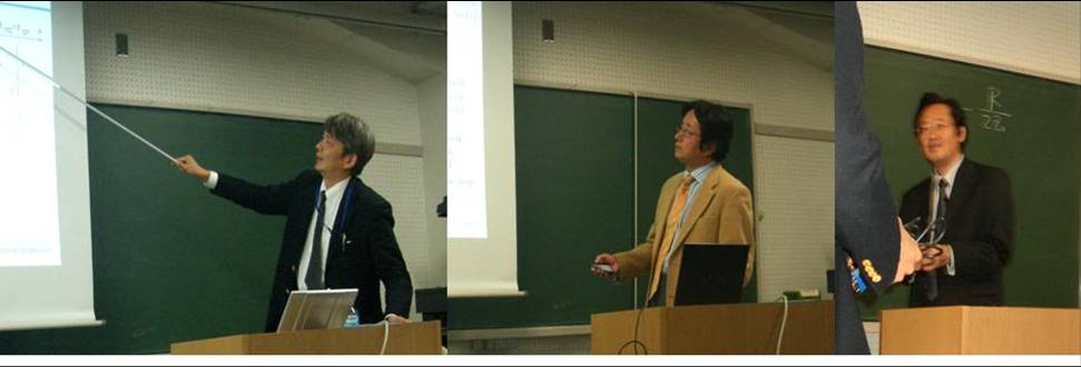
On Nov. 28, 2007, the DL meeting was held at the Ookayama Campus of Tokyo Institute of Technology, Tokyo. Three Japanese DLs, all from Tokyo Institute of Technology, gave presentations on novel interesting technologies. Prof. Yasuyuki Miyamoto talked about high mobility transistors using electron launching in heterostructures. The title of his talk was "Gate controlled hot-electron transistors." Prof. Sunri Oda lectured on "Silicon nanocrystal devices." In his talk, single electron devices and their quantum effects were detailed with regard to future memory devices. Prof. Kazuya Masu gave a presentation on GHz interconnect technology in Si ULSI in order to achieve high speed and low power consumption for global interconnect. The title was "Wiring technologies for on-chip transmission line." Each lecture was followed by fruitful discussions between the lecturer and the audience. The meeting offered the more than 20 attendees the opportunity to get grips with interesting recent research activities.
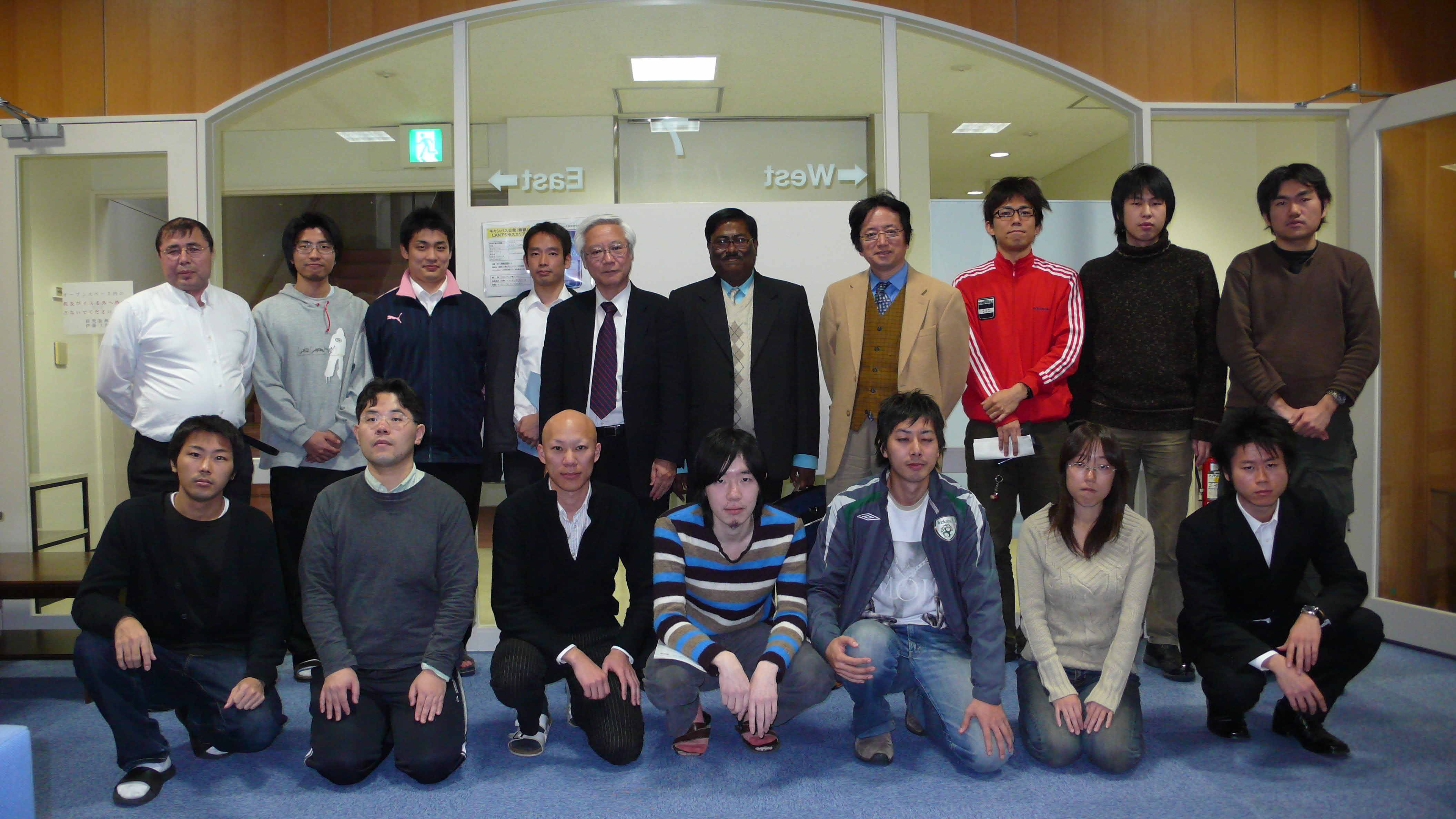
The third DL meeting was held on Nov. 29, 2007. A talk entitled "Nanoelectronic devices based on silicon MOS structures" was given by Prof. C. K. Sarkar of Jadavpur University, Kolkata, India, at the Suzukakedai Campus of Tokyo Institute of Technology, Yokohama. His talk focused on the performance of nanocrystallites and nanotubes with embedded gate oxides having different dielectric constants of submicron MOS. The meeting was very successful with 20 participants.
In addition, in the latter half of the year from July 2007 to Dec. 2007, ED Japan Chapter had 6 joint technical meetings with the Japan Society of Applied Physics, the Institute of Electronics, Information and Communication Engineers, etc.
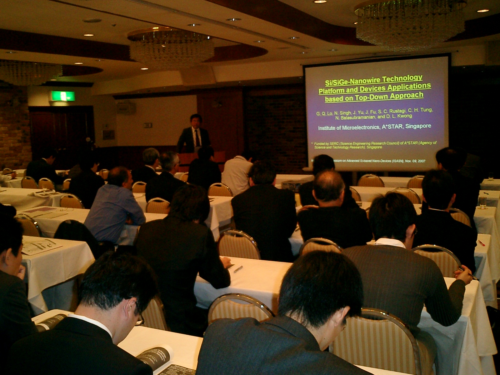
International Symposium on Advanced Si-based Nanodevices (ISASN) on Nov. 9, 2007. The Symposium was held at Toranomon Pastoral, Tokyo, Japan.
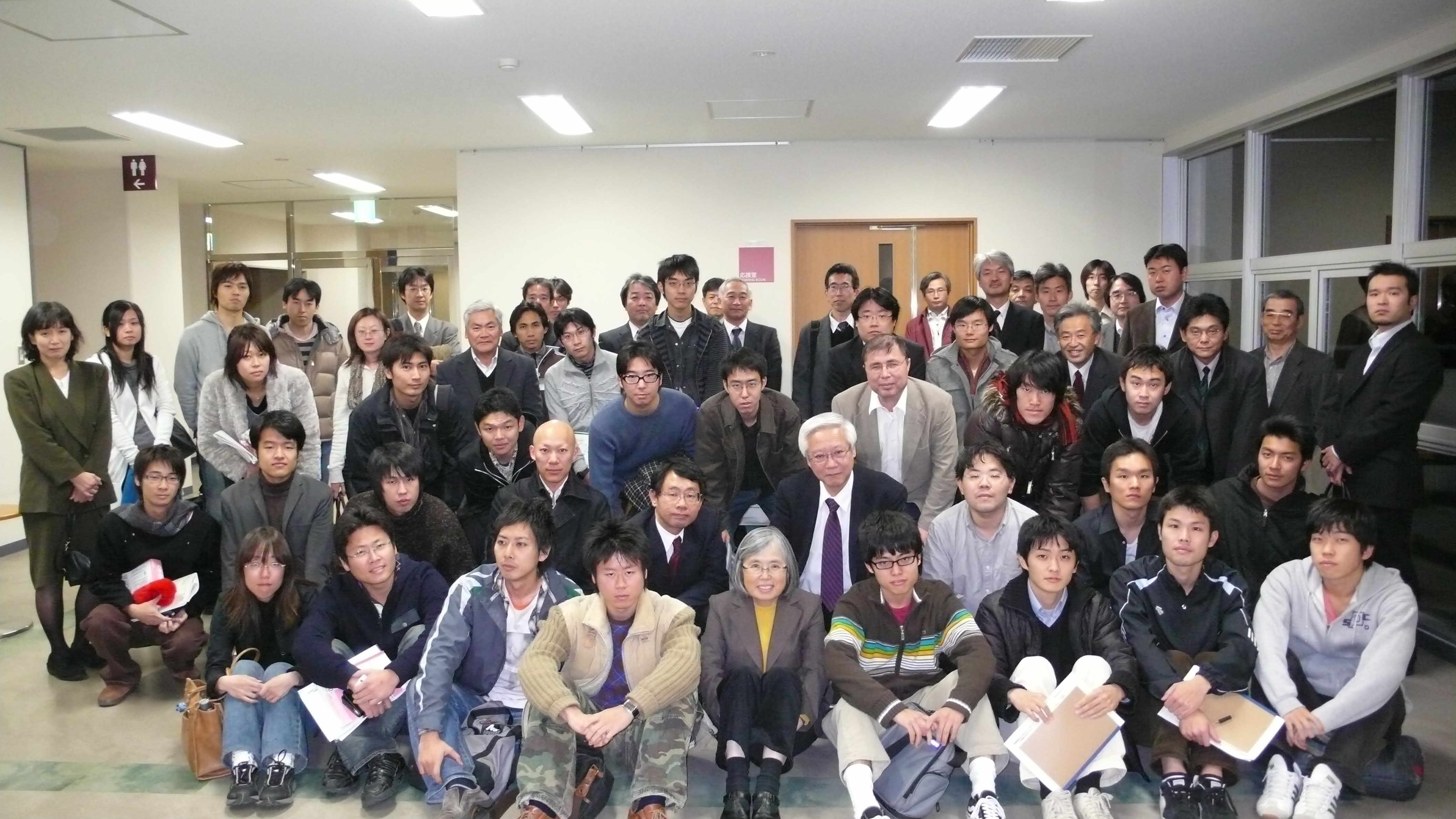
Prof. Mitiko Miura-Mattausch (at the center at the front) and the audience at the DL meeting on Nov. 19, 2007.
The DL meeting on Nov. 28, 2007. Three Japanese DLs; from the left: Prof. Yasuyuki. Miyamoto, Prof. Synri Oda, Prof. Kazuya Masu.
The DL meeting on Nov. 29, 2007. From the fifth person from the left at the back: Prof. Hiroshi Iwai, Partner and EDS Jr. Past President, Prof. C. K. Sarkar of Jadavpur University, India,, Prof. Synri Oda of Tokyo Institute of Technology.