EDS Newsletter: January 2008
On July 12, 2007, ED Japan Chapter organized a technical meeting entitled “Possibility of controlling variations in semiconductor device behaviors: How do we model the variations?,” which was held at Hiroshima University, Hiroshima, Japan. Recently, the “variation control” is one of the hottest R&D issues of semiconductor devices, and the meeting offered the attendees the opportunity to obtain the latest information. Six speakers gave presentations on their topics from the viewpoint of either the device development or the circuit design.
Firstly, Prof. Mitiko Miura-Mattausch of Hiroshima Univ. gave a DL lecture to overview the current status of the circuit variation analysis and its future applications. The title of her talk was “Status of device modeling technology: Toward analyzing and predicting the variations among integrated circuits.”
From the device development point of view, three talks were given. Dr. Ken-ichiro Sonoda of Renesas Technology gave a presentation on “Statistical analysis and modeling of Random Telegraph Signal (RTS) in small-geometry MOSFETs.” Dr. Tetsufumi Tanamoto of Toshiba discussed the quantum effect in future MOSFETs in a talk entitled “Fluctuation of ballistic conduction current caused by electron traps in the Kondo regime.” An interesting talk on “A methodology to optimize device structures using TCAD” was given by Dr. Koichi Fukuda of Oki Electric Industry.
In the latter half of the meeting, Prof. Hans Juergen Mattausch of Hiroshima Univ. discussed the latest results of variation analysis from the circuit designers viewpoint in a presentation entitled “Circuit-variation analysis based on device/process variations.” Dr. Yoshihisa Iino of Silvaco Japan gave a talk on “An EDA platform linking ‘variation’ and ‘computer simulation.’”
All the speakers engaged in lively and fruitful discussions with the audience. This meeting, which was attended by more than 100 people, was very beneficial for chapter members and was a great success.
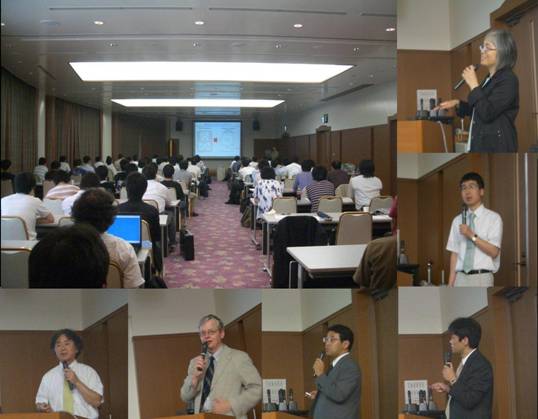
More than 100 people attended the ED Japan Chapter technical meeting held at Hiroshima Univ. on July 12, 2007. Six speakers including Prof. Miura, an EDS DL, gave presentations on the latest developments in device modeling.