IEEE Electron Devices Society ~Japan Joint Chapter~
Home About Us Meetings Newsletter Awards Committee Links
IEEE EDS
IEEE EDS Japan Joint Chapterは、学生研究者の学会活動を奨励し研究活動を活性化するために、2002年にJapan Chapter
Student Awardを創設致しました。
本賞は、日本国内の大学、大学院に所属する若い学生研究者のなかで、電子デバイス技術への貢献が優れて大きいと認められる方に授与されます。具体的には、EDS主催の重要国際学会において、第一著者として口頭発表された学生研究者の中から、毎年12月に、数名の受賞者を選考致します。尚、主要学会での発表状況は、チャプター役員あるいはチャプターが委嘱した審査員が把握しておりますので、本賞への自薦・他薦は受け付けておりません。
また、対象者はIEEE EDS学生会員あるいは、本賞授与時までに入会申請手続きをとって頂ける方になります。学生会員入会手続きはIEEE東京支部のホームページをご参考下さい。
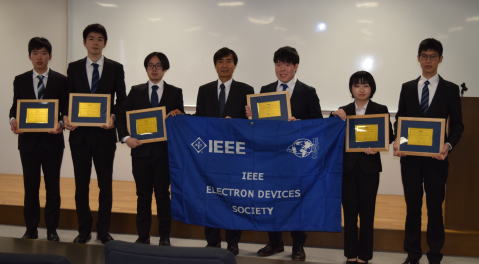
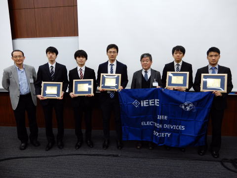
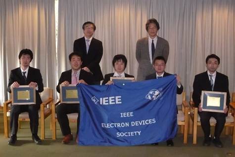
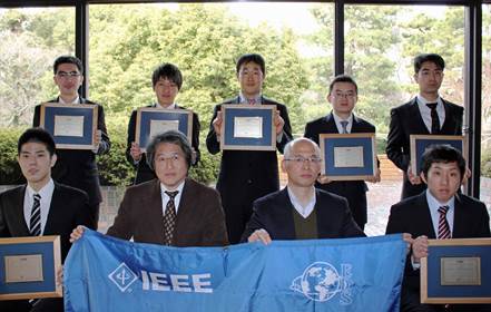
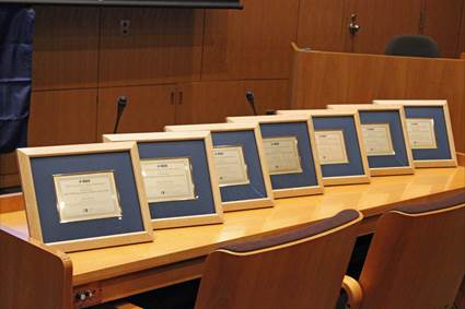
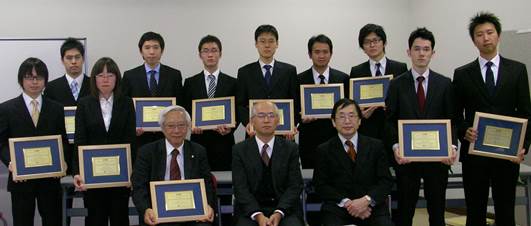
表彰式は、毎年1月のチャプター総会において挙行され、受賞者には、賞状盾が授与されます。
IEEE EDS Japan Chapter Student Award (VLSI)
| Masaki Abe, Chuo University “Pre-shipment Data-retention/Read-disturb Lifetime Prediction & Aftermarket Cell Error Detection & Correction by Neural Network for 3D-TLC NAND Flash Memory” |
| Chengji Jin, The University of Tokyo “Transient Negative Capacitance as Cause of Reverse Drain-induced Barrier Lowering and Negative Differential Resistance in Ferroelectric FETs” |
| Tsung-En Lee, The University of Tokyo “Improvement of SiGe MOS interface properties with a wide range of Ge contents by using TiN/Y2O3 gate stacks with TMA passivation” |
| Fei Mo, The University of Tokyo “Experimental Demonstration of Ferroelectric HfO2 FET with Ultrathin-body IGZO for High-Density and Low-Power Memory Application” |
IEEE EDS Japan Chapter Student Award (IEDM)
| Kanako Ando, Kagawa University “Highly Sensitive Silicon Slip Sensing Imager for Forceps Grippers Used under Low Friction Condition” |
| Takuya Maeda, Kyoto University “Impact Ionization Coefficients in GaN Measured by Above- and Sub-Eg Illuminations for p−/n+ Junction” |
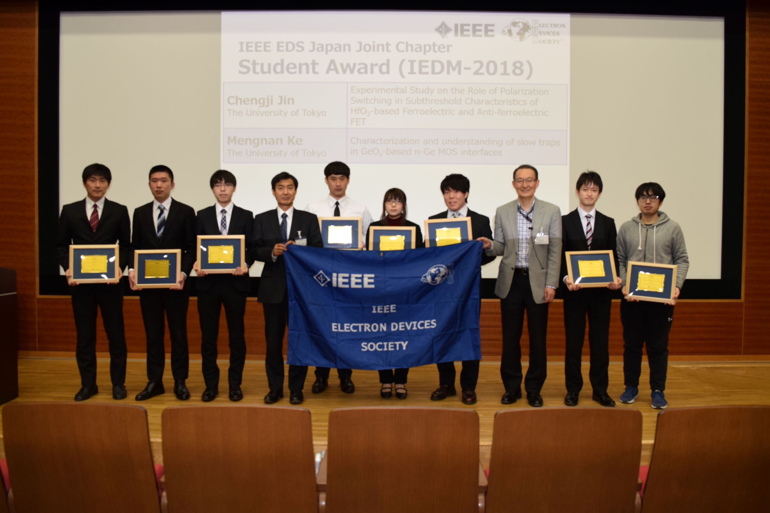
第17回 2018年IEEE EDS Student Award(2019年1月25日授与)
IEEE EDS Japan Chapter Student Award (VLSI)
| Yusuke Yamaga, Chuo University 5x Reliability Enhanced 40nm TaOx Approximate-ReRAM with Domain-Specific Computing for Real-time Image Recognition of IoT Edge Devices |
| Kwang-Won Jo, The University of Tokyo Hole mobility enhancement in extremely-thin-body strained GOI and SGOI pMOSFETs by improved Ge condensation method |
IEEE EDS Japan Chapter Student Award (IEDM)
| Maasa Murata, Tohoku University A 24.3Me- Full Well Capacity CMOS Image Sensor with Lateral Overflow Integration Trench Capacitor for High Precision Near Infrared Absorption Imaging |
| Fei Mo, The University of Tokyo Scalability Study on Ferroelectric-HfO2 Tunnel Junction Memory Based on Non-equilibrium Green Function Method with Self-consistent Potential |
| Masahiro Yamamoto, Tohoku University A CMOS Proximity Capacitance Image Sensor with 16um Pixel Pitch, 0.1aF Detection Accuracy and 60 Frames Per Second |
| Takuya Maeda, Kyoto University Parallel-Plane Breakdown Fields of 2.8-3.5 MV/cm in GaN-on-GaN p-n Junction Diodes with Double-Side-Depleted Shallow Bevel Termination |
| Chengji Jin, The University of Tokyo Experimental Study on the Role of Polarization Switching in Subthreshold Characteristics of HfO2-based Ferroelectric and Anti-ferroelectric FET |
| Mengnan Ke, The University of Tokyo Characterization and understanding of slow traps in GeOx-based n-Ge MOS interfaces |
第16回 2017年IEEE EDS Student Award(2018年2月2日授与)
IEEE EDS Japan Chapter Student Award (VLSI)
| Hiroshi Oka, Osaka University Enhancement-mode n-channel TFT and Room-temperature Near-infrared Emission Based on n+/p junction in Single-crystalline GeSn on Transparent Substrate |
| Masashi Haraguchi, Keio University A 6Gb/s Rotatable Non-Contact Connector withHigh-Speed/I2C/CAN/SPI Interface Bridge IC |
| Wu-Kang Kim, The University of Tokyo High Performance 4.5-nm-Thick Compressively-Strained Ge-on-Insulator pMOSFETs Fabricated by Ge Condensation with Optimized Temperature Control |
| Yoshiaki Deguchi, Chuo University Flash Reliability Boost Huffman Coding (FRBH): Co-Optimization of Data Compressionand VTH Distribution Modulation to Enhance Data-Retention Time by over 2900x |
IEEE EDS Japan Chapter Student Award (IEDM)
| Kyoji Mizoguchi, Chuo University Lateral Charge Migration Suppression of 3D-NAND Flash by Vth Nearing for Near Data Computing |
| Xuan Tian, The University of Tokyo Sub-nm EOT Ferroelectric HfO2 on p+Ge with Highly Reliable Field Cycling Properties |
第15回 2016年IEEE EDS Student Award(2017年2月15日授与)
IEEE EDS Japan Chapter Student Award (VLSI)
| Dae-Hwan Ahn (The University of Tokyo) Performance improvement of InxGa1‐xAs Tunnel FETs with Quantum Well and EOT scaling |
| Atsuro Kobayashii (Chuo University) Versatile TLC NAND Flash Memory Control to Reduce Read Disturb Errors by 85% and Extend Read Cycles by 6.7‐times of Read‐Hot and Cold Data for Cloud Data Centersi |
| Hidetake Sugo (Tohoku University) A Dead-time Free Global Shutter CMOS Image Sensor with in-pixel LOFIC and ADC using Pixel-wise Connections |
| Sho Ikeda (Tokyo Institute of Technology) An 8.865‐GHz ‐244dB‐FOM High‐Frequency Piezoelectric Resonator‐Based Cascaded Fractional‐N PLL with Sub‐ppb‐Order Channel Adjusting Technique |
IEEE EDS Japan Chapter Student Award (IEDM)
| Manabu Suzuki (Tohoku University) An Over 1Mfps Global Shutter CMOS Image Sensor with 480 Frame Storage Using Vertical Analog Memory Integration |
|
Junjie An (University of Tsukuba) Experimental Demonstration of -730V Vertical SiC p-MOSFET with High Short Circuit Withstand Capability for Complementary Inverter Applications |
| Chih-Yu Changi (The University of Tokyo) Impact of La2O3/InGaAs MOS Interface on InGaAs MOSFET Performance and its Application to InGaAs Negative Capacitance FET |
| Hiroshi Oka (Osaka University) High-mobility TFT and Enhanced Luminescence Utilizing Nucleation-controlled GeSn Growth on Transparent substrate for Monolithic Optoelectronic Integration |
| Lun Xu (The University of Tokyo) General Relationship for Cation and Anion Doping Effects on Ferroelectric HfO2 Formation |
| Jae-Hoon Han (The University of Tokyo) Extremely High Modulation Efficiency III-V/Si hybrid MOS Optical Modulator Fabricated by Direct Wafer Bonding |
第14回 2015年IEEE EDS Student Award(2016年2月9日授与)
IEEE EDS Japan Chapter Student Award (VLSI)
-
Cimang Lu (東京大学)
Design and Demonstration of Reliability-aware Ge Gate Stacks with 0.5 nm EOTKoichi Nishi (東京大学)
High Hole Mobility Front-gate InAs/InGaSb-OI Single Structure CMOS on Si
Hao Qiu (東京大学)
Impact of Random Telegraph Noise on Write Stability in Silicon-on-Thin-BOX (SOTB) SRAM Cells at Low Supply Voltage in Sub-0.4V RegimeSenju Yamazaki(中央大学)
Reliability Enhancement of 1X nm TLC for Cold Flash and Millennium Memories
-
Xiao Yu (東京大学)
Experimental Study on Carrier Transport Properties in Extremely-Thin Body Ge-on-Insulator (GOI) p-MOSFETs with GOI Thickness Down to 2 nmXiuyan Li (東京大学)
Self-decomposition of SiO2 due to Si-chemical Potential Increase in SiO2 between HfO2 and Substrate – Comprehensive Understanding of SiO2-IL Scavenging in HfO2 Gate Stacks on Si, SiGe and SiC –
Shoichi Kabuyanagi (東京大学)
Effects of Free-carriers on Rigid Band and Bond Descriptions in Germanium – Key to Designing and Modeling in Ge Nano-devices –
第13回 2014年 IEEE EDS Student Award (2015年2月12日授与)
IEEE EDS Japan Chapter Student Award
(VLSI)
Sheyang Ning (東京大学、中央大学)
“23% Faster Program and 40% Energy
Reduction of
Sang Hyeon Kim (東京大学)
“High Performance
InGaAs-On-Insulator MOSFETs on Si by Novel Direct
Akitsugu Ueda
“Ultra-Low Voltage (0.1V) Operation of Vth Self-Adjusting MOSFET and SRAM Cell”
IEEE EDS Japan Chapter Student Award
(IEDM)
Xiuyan Li (東京大学)
“Analytical Formulation of SiO2-IL
Scavenging in HfO2/SiO2/Si Gate Stacks:A Key is the SiO2/Si
Interface Reaction”
Minsoo Kim (東京大学)
“High Ion/Ioff
Ge-source Ultrathin Body Strained-SOI Tunnel FETs – Impact of Channel Strain,
MOS Interfaces and Back Gate on the Electrical Properties”
Akito Suzuki
“Source-induced RDF Overwhelms RTN in Nanowire Transistor: Statistical Analysis
with Full Device EMC/MD Simulation Accelerated by GPU Computing”
第12回 2013年 IEEE EDS Student Award (2014年2月3日授与)
IEEE EDS Japan Chapter Student Award
(VLSI)
Choong Hyun Lee (東京大学)
“Enhancement of High-Ns Electron
Mobility in Sub-nm EOT Ge n-MOSFETs”
Sang Hyeon Kim (東京大学)
“Strained Extremely-Thin Body In0.53Ga0.47As-On-Insulator
MOSFET on Si Substrates” and
“High Performance Extremely-Thin Body InAs-On-Insulator MOSFETs on Si with Ni-InGaAs
Metal S/D by Contact Resistance Reduction Technology”
IEEE EDS Japan Chapter Student Award
(IEDM)
Dariush Hassan Zadeh (東京工業大学)
“Low Dit
High-k/In0.53Ga0.47As Gate Stack, with CET Down to 0.73
nm and Thermally Stable Silicide Contact by Suppression of Interfacial
Reaction”
Go Oike (東京大学)
“High Electron Mobility (>16 cm2/Vsec) FETs with High On/Off Ratio (>106) and
Highly Conductive Films (σ>102 S/cm) by Chemical Doping in Very
Thin (~20 nm) TiO2 Films on Thermally Grown SiO2”
Muneki Akazawa (広島大学)
“Local Transfer of Single-Crystalline
Silicon (100) Layer by Meniscus Force and Its Application to High-Performance
MOSFET Fabrication on Glass Substrate”
Shunsuke Koba (神戸大学)
“The Impact of Increased Deformation
Potential at MOS Interface on Quasi-Ballistic Transport in Ultrathin Channel
MOSFETs Scaled down to Sub-10 nm Channel Length”
Munetaka Noguchi (東京大学)
“High Ion/Ioff
and Low Subthreshold Slope Planar-Type InGaAs Tunnel FETs with Zn-Diffused Source Junctions”
IEEE EDS Japan Chapter Student Award
(VLSI)
Rui Zhang (東京大学)
“High Mobility Ge
pMOSFETs with 0.7 nm Ultrathin EOT using HfO2/Al2O3/GeOx/Ge Gate Stacks Fabricated by
Plasma Post Oxidation”
SangHyeon Kim (東京大学)
“Sub-60
nm Deeply-Scaled Channel Length Extremely-thin Body InxGa1-xAs-On-Insulator
MOSFETs on a Si with Ni-InGaAs Metal S/D and MOS
Interface Buffer Engineering”
IEEE EDS Japan Chapter Student Award
(IEDM)
Kentaro Kukita (大阪大学)
“Impact of Quasi-Ballistic Phonon Transport
on Thermal Properties in Nanoscale Devices: A Monte
Carlo Approach”
Takashi Matsumoto (京都大学)
“Impact of Random Telegraph Noise on CMOS
Logic Delay Uncertainty under Low Voltage Operation”
Nobuyasu Beppu (東京工業大学)
“Experimental Study of Self-Heating Effect
(SHE) in SOI MOSFETs: Accurate Understanding of Temperatures During AC
Conductance Measurement, Proposals of 2ω Method and Modified Pulsed IV”
IEEE EDS Japan Chapter Student Award
(VLSI)
Rui Zhang (東京大学)
“High Mobility Ge
pMOSFETs with ~1nm Thin EOT Using Al2O3/GeOx/Ge Gate Stacks Fabricated by
Plasma Post Oxidation”
SangHyeon Kim (東京大学)
“High Performance Extremely-Thin Body
III-V-On-Insulator MOSFETs on a Si Substrate with Ni-InGaAs
Metal S/D and MOS Interface Buffer Engineering”
Yasuhiro Nakajima (東京大学)
“Phase Transformation Kinetics of HfO2
Polymorphs in Ultra-Thin Region”
IEEE EDS Japan Chapter Student Award
(IEDM)
Yoshiharu Yonai (東京工業大学)
“High drain current (>2A/mm) InGaAs channel MOSFET at VD=0.5V with shrinkage
of channel length by InP”
Teruyuki Ohashi (東京工業大学)
“Experimental Evidence of Increased
Deformation Potential at MOS Interface and Its Impact on Characteristics of
ETSOI FETs”
Tsunaki Takahashi (東京工業大学)
“Thermal-Aware Device Design of Nanoscale Bulk/SOI FinFETs: Suppression
of Operation Temperature and Its Variability”
Tomoyuki Yokota (東京大学)
“Sheet-type Organic Active Matrix
Amplifier System using Vth-Tunable,
Pseudo-CMOS Circuits with Floating-gate Structure”
 |
 |
||
歴代受賞者 (敬称略、50音順)
2010年 第9回
Naotoshi Kadotani 角谷 直哉 (東京工業大学)
“Anomalous
Electron Mobility in Extremely-Thin SOI (ETSOI) Diffusion Layers with SOI
Thickness of Less Than 10 nm and High Doping Concentration of Greater Than 1x1018cm-3” (2010 IEDM)
Sang Hyeon Kim 金 相賢(東京大学)
“Self-aligned
Metal Source/Drain InxGa1-xAs n-MOSFETs Using Ni-InGaAs Alloy” (2010 IEDM)
Choong Hyun Lee 李 忠賢 (東京大学)
“Ge MOSFETs
Performance: Impact of Ge Interface Passivation” (2010 IEDM)
Xiaowei Song 宋 驍嵬 (東京大学)
“Impact of DIBL Variability on SRAM
Static Noise Margin Analyzed by DMA SRAM TEG” (2010 IEDM)
Makoto Suzuki 鈴木 誠 (東京大学)
“Direct
Measurements, Analysis, and Post-Fabrication Improvement of Noise Margins in
SRAM Cells Utilizing DMA SRAM TEG” (2010 Symp. on VLSI Technology)
Kiichi Tachi 舘 喜一 (東京工業大学)
“Experimental
Study on Carrier Transport Limiting Phenomena in 10 nm Width Nanowire CMOS
Transistors” (2010 IEDM)
Keita Yamaguchi
山口 慶太 (筑波大学)
“Universal
Guiding Principle for the Fabrication of Highly Scalable MONOS-Type Memories
-Atomistic Recipes Based on Designing Interface Oxygen Chemical Potential-” (2010 IEDM)
2009年 第8回
受賞者: Miyuki Kouda 幸田 みゆき (東京工業大学)
“Charged Defects Reduction in Gate Insulator with Multivalent Materials” (2009 Symp. on VLSI Technology)
受賞者: Ken
Shimizu 清水 健 (東京大学)
“Physical Understandings of Si (110) Hole Mobility in Ultra-Thin Body pFETs by <110> and <111> Uniaxial Compressive
Strain” (2009 IEDM)
受賞者: Makoto Suzuki 鈴木 誠 (東京大学)
“Post-Fabrication Self-Convergence Scheme for Suppressing Variability in SRAM
Cells and Logic Transistors” (2009 Symp. on VLSI
Technology)
受賞者: Tsunaki Takahashi 高橋 綱己 (東京工業大学)
“Direct Observation of Subband Structures in (110) pMOSFETs under High Magnetic Field: Impact of Energy Split
Between Bands and Effective Masses on Hole Mobility” (2009 IEDM)
受賞者: Kiichi Tachi 舘 喜一 (東京工業大学)
“Relationship Between Mobility and High-k Interface Properties in Advanced Si
and SiGe Nanowires” (2009 IEDM)
受賞者: Shuhei Tanakamaru 田中丸 周平 (東京大学)
“A 0.5V Operation, 32% Lower Active Power, 42% Lower Leakage Current,
Ferroelectric 6T-SRAM with VTH Self-Adjusting Function for 60% Larger Static
Noise Margin” (2009 IEDM)
受賞者: Jiezhi Chen 陳 杰智 (東京大学)
“High Hole Mobility in Multiple Silicon Nanowire Gate-All-Around pMOSFETs on (110) SOI” (2009 Symp. on VLSI Technology)
受賞者: Kohei Nakanishi 中西 洸平 (筑波大学)
“Self-Consistent Monte Carlo Device Simulations Under Nano-Scale Device
Structures: Role of Coulomb Interaction, Degeneracy, and Boundary Condition” (2009 IEDM)
受賞者: Arifin Tamsir Putra (東京大学)
“A New Methodology for Evaluating VT Variability Considering Dopant Depth
Profile” (2009 Symp. on VLSI Technology)
受賞者: Kiyohito Morii 森井 清仁 (東京大学)
“High Performance GeO₂/Ge nMOSFETs with Source/Drain Junctions Formed by Gas Phase
Doping” (2009 IEDM)
受賞者: Keita Yamaguchi 山口 慶太(筑波大学)
“Atomistic Guiding Principles for MONOS-Type Memories with High Program/Erase
Cycle Endurance” (2009 IEDM)
受賞者: Choong Hyun Lee 李 忠賢(東京大学)
“Record-high Electron Mobility in Ge n-MOSFETs Exceeding Si Universality” (2009 IEDM)
2008年 第7回
受賞者: Yusaku
Kato 加藤 祐作 (東京大学)
"A Large-Area,
Flexible, Ultrasonic Imaging System With A Printed Organic Transistor Active
Matrix " (2008 IEDM)
受賞者: Shoma Kuga 久我 翔馬 (早稲田大学)
"Precise
Detection Of Single Mismatched DNA With Functionalized Diamond Electrolyte
Solution Gate FET" (2008 IEDM)
受賞者: Ken Shimizu 清水 健 (東京大学)
"Experimental Investigation on the
Origin of Direction Dependence of Si(110) Hole Mobility Utilizing Ultra-Thin
Body pMOSFETs " (2008 IEDM)
受賞者: Jiezhi Chen (東京大学)
"Experimental Study of Mobility in
[110]- and [100]-Directed Multiple Silicon Nanowire GAA MOSFETs on (100)
SOI" (2008 Symp. on VLSI Technology)
受賞者: Yousuke Nakakita 中北 要佑 (東京大学)
"Interface-Controlled Self-Align
Source/Drain Ge pMOSFETs
Using Thermally-Oxidized GeO2 Interfacial Layers" (2008 IEDM)
受賞者: Yeon-Joo Jeong (東京大学)
“Uniaxial
Strain Effects on Silicon Nanowire pMOSFET and
Single-Hole Transistor at Room Temperature” (2008 IEDM)
2007年 第6回
受賞者: Kenichi Abe 阿部 健一 (東北大学)
"Random Telegraph Signal Statistical
Analysis using a Very Large-Scale Array TEG with 1M MOSFETs” (2007 Symp. On VLSI
Technology)
受賞者: Ken Shimizu 清水 健 (東京大学)
"
Mobility Enhancement in Uniaxially Strained (110)
Oriented Ultra-Thin Body Single- and Double-Gate MOSFETs with SOI
Thickness of Less Than 4 nm " (2007 IEDM)
受賞者: Toshitake Takahashi 高橋 俊岳 (東京大学)
"
Proof of Ge-Interfacing Concepts for Metal/High-k/Ge CMOS -- Ge-Intimate Material Selection and
Interface Conscious Process Flow --” (2007 IEDM)
受賞者: Kazuyuki Hirama 平間 一行 (早稲田大学)
"
High-Performance P-Channel Diamond MOSFETs with Alumina Gate Insulator” (2007 IEDM)
2006年 第5回
大藤徹(東京大学)、小林正治(東京大学)
2005年 第4回
加藤祐作(東京大学)、上村崇史(大阪大学)、黒田理人(東北大学)、筒井元(東京大学)、山村 傑(大阪大学)
2004年 第3回
伊藤浩之(東京工業大学)、入江宏(東京大学)、上村崇史(大阪大学)、河野剛士(豊橋技術科学大学)、齋藤真澄(東京大学)
2003年 第2回
石川寧(東北大学)、入江宏(東京大学)、上村崇史(筑波大学)、齋藤真澄(東京大学)
2002年 第1回
天野建(東京工業大学)、小林大輔(東京大学)、齋藤真澄(東京大学)、中辻広志(大阪大学)、細井卓治(大阪大学)