日時
会場
主催
共催
講演
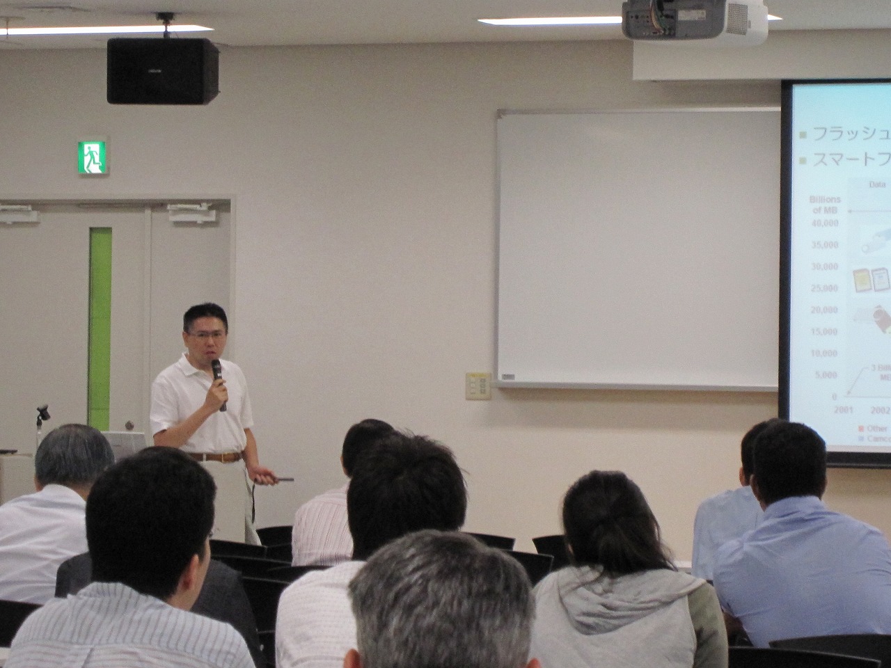
Kunihiko Iizuka, SHARP Corporation, IEEE SSCS Kansai Chapter Chair
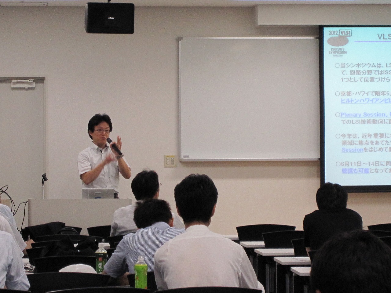 VLSI Symposium 2012 Review Talk
Hideyuki Kabuo, Panasonic Corporation, VLSI Symposium 2012, Program committee Co-Chair
 "A 0.45-V Input On-Chip Gate Boosted (OGB) Buck
Converter in 40-nm CMOS with More Than 90% Efficiency in Load Range from
2uW to 50uW"
"A 0.45-V Input On-Chip Gate Boosted (OGB) Buck
Converter in 40-nm CMOS with More Than 90% Efficiency in Load Range from
2uW to 50uW"Xin Zhang, P.-H. Chen, Y. Ryu*, K. Ishida, Y. Okuma*, K. Watanabe*, T. Sakurai, M. Takamiya, University of Tokyo, *STARC
A 0.45-V input, 0.4-V output on-chip gate boosted (OGB) buck converter with clock gated digital PWM controller in 40-nm CMOS achieved the highest efficiency to date with the output power less than 40uW. A linear delay trimming by a logarithmic stress voltage (LSV) scheme to compensate for the die-to-die delay variations of a delay line in the PWM controller with good controllability is also proposed.
 "A 0.41μA Standby Leakage 32Kb Embedded SRAM
with Low-Voltage Resume-Standby utilizing All Digital Current Comparator
in 28nm HKMG"
"A 0.41μA Standby Leakage 32Kb Embedded SRAM
with Low-Voltage Resume-Standby utilizing All Digital Current Comparator
in 28nm HKMG"Noriaki Maeda, S. Komatsu, M. Morimoto, Y. Shimazaki, Renesas Electronics
A high-performance and low-leakage current embedded SRAM for mobile phones is proposed. The proposed SRAM has a low-voltage resume-standby mode to reduce the standby leakage. An all digital current comparator is also proposed to choose a suitable standby mode. A test chip was fabricated using 28 nm HKMG CMOS technology. The proposed 32 Kb SRAM has a 0.41 μA standby leakage which is the conventional half, with 420 ps access.
 "x11 Performance Increase, x6.9 Endurance
Enhancement, 93% Energy Reduction of 3D TSV-Integrated Hybrid ReRAM/MLC
NAND SSDs by Data Fragmentation Suppression"
"x11 Performance Increase, x6.9 Endurance
Enhancement, 93% Energy Reduction of 3D TSV-Integrated Hybrid ReRAM/MLC
NAND SSDs by Data Fragmentation Suppression"H. Fujii, K. Miyaji, K. Johguchi, K. Higuchi, C. Sun, Ken Takeuchi, Chuo University
A 3D through-silicon-via (TSV) -integrated hybrid ReRAM/multi-level-cell (MLC) NAND solid-state drives (SSDs) architecture is proposed for PC, server and smart phone applications. NAND-like interface and sector-access overwrite policy are proposed for the ReRAM. Furthermore, three intelligent data management algorithms (anti-fragmentation, most-recently-used and reconsidered-as-a-fragmentation algorithms) are proposed. The proposed algorithms suppress data fragmentation and excess usage of the MLC NAND by storing hot data in the ReRAM. As a result, 11 times performance increase, 6.9 times endurance enhancement and 93% write energy reduction are achieved compared with the conventional MLC NAND SSD. Both ReRAM write and read latency should be less than 3us to obtain these improvements. The Required endurance for ReRAM is 1e5. 3D TSV interconnects reduce the energy consumption by 68%.
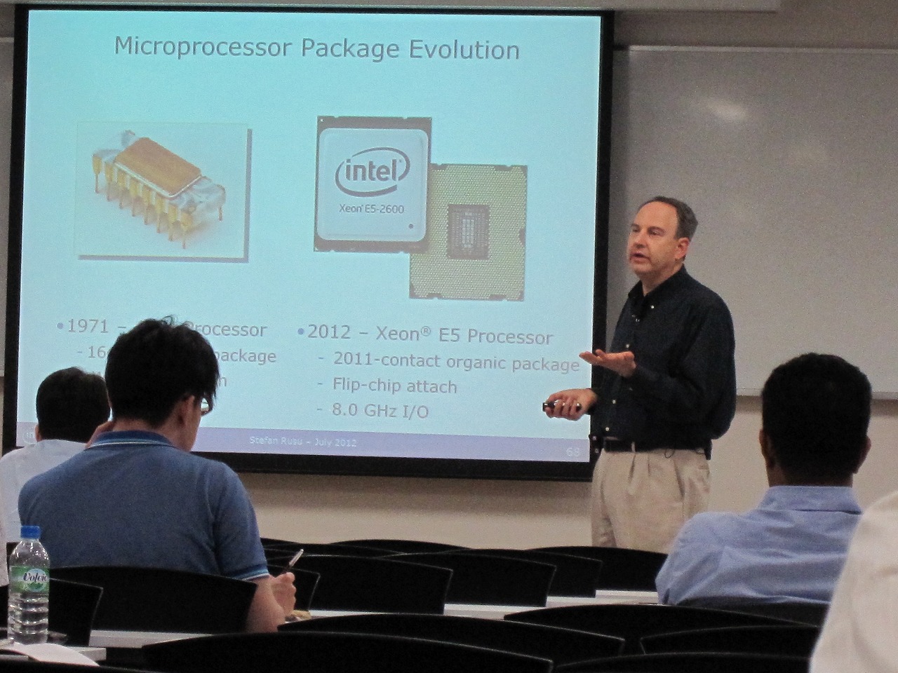 "Microprocessor Design in the Nanoscale Era" PDF(4.7MB)
Stefan Rusu, Intel Corporation
Moore's Law has fueled the worldwide technology revolution for over 40 years and will continue to drive higher feature integration in leading-edge microprocessors with multiple cores and larger on-die caches. CMOS process technology will continue its historical scaling trend, while research activities are focusing on novel devices and manufacturing techniques. Process, voltage and temperature variations are driving a paradigm shift from a deterministic to a probabilistic design methodology. Active and leakage power will remain the main limiters for both server and client processors. This presentation will review several techniques to control switching power and leakage with practical examples from Intel designs. Continued improvements in packaging technology enhance the cooling capabilities, while providing better power delivery and higher pin counts.
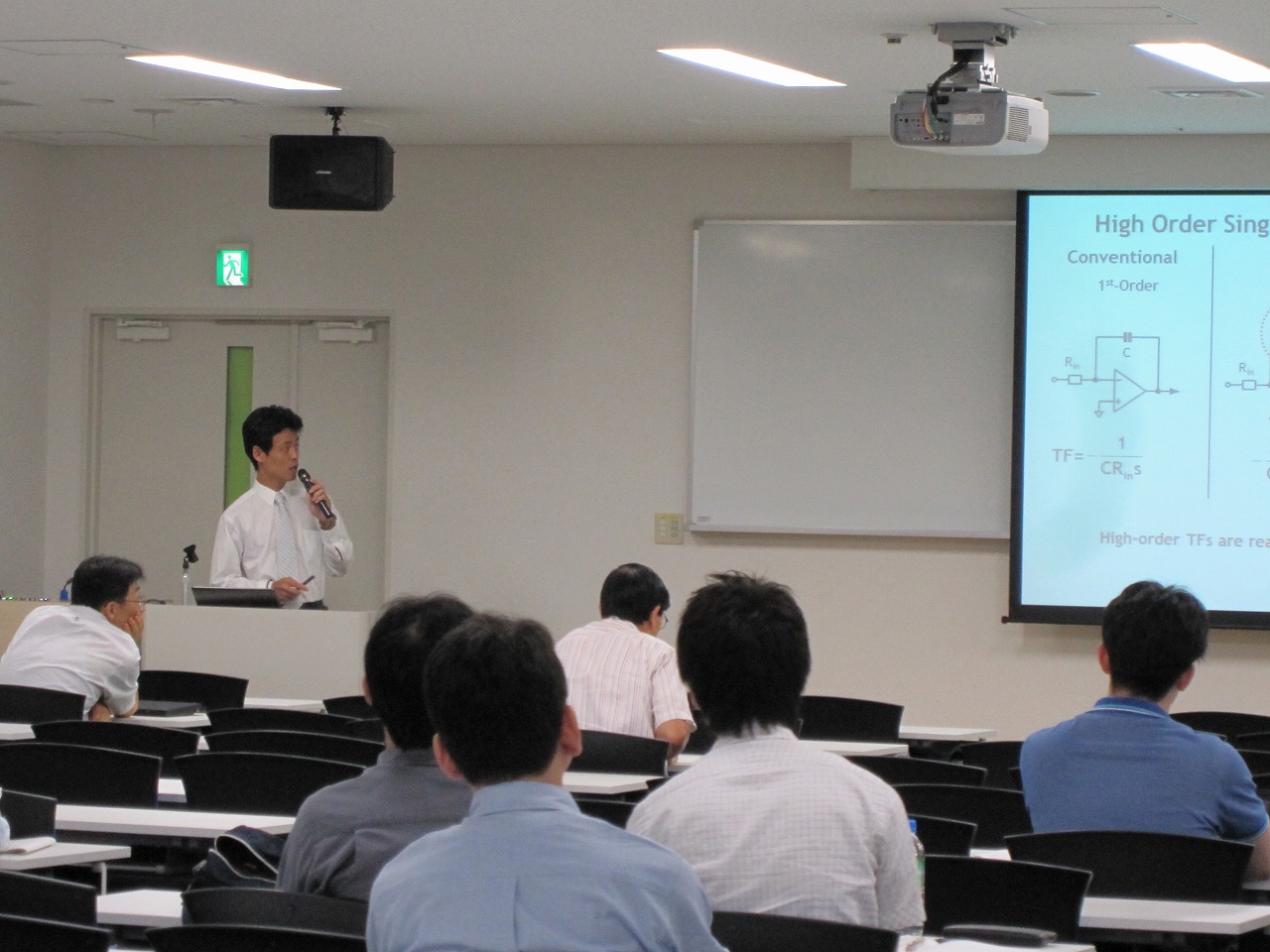 "A 50 fJ/conv. Continuous Time delta-sigma
Modulator with High-order Single Opamp Integrator using Optimization-based
Design Method"
"A 50 fJ/conv. Continuous Time delta-sigma
Modulator with High-order Single Opamp Integrator using Optimization-based
Design Method"Kazuo Matsukawa, K. Obata, Y. Mitani, S. Dosho, Panasonic Corporation
We propose not only new power and area efficient circuit configurations but also an optimization design method for such configurations. So far, design difficulties of the modulator, such as a trade-off between loop stability and a performance and unknown distortion mechanism, have been serious obstacles to improve the efficiency. Major factors to overcome these obstacles are new high-order single opamp integrators using optimization-based design method and tuning systems for harmonic distortions. Two design examples for TV-tuner application confirm that those design approach can maximize the performance of various types of modulators. A simple 3rd-order modulator achieved the FOM of 101 fJ/conv. and more complex 4th-order one achieved 50 fJ/conv. which is less than half of ever reported.
 "A 61-dB SNDR 700 μm2 Second-Order All-Digital
TDC with Low-Jitter Frequency Shift Oscillators and Dynamic
Flipflops"
"A 61-dB SNDR 700 μm2 Second-Order All-Digital
TDC with Low-Jitter Frequency Shift Oscillators and Dynamic
Flipflops"Toshihiro Konishi, K. Okuno, S. Izumi, M. Yoshimoto, H. Kawaguchi, Kobe University
We present a small-area second-order all-digital time-to-digital converter (TDC) with two frequency shift oscillators (FSOs) comprising inverter chains and dynamic flipflops featuring low jitter. The proposed FSOs can maintain their phase states through continuous oscillation, unlike conventional gated ring oscillators (GROs) that are affected by transistor leakage. Our proposed FSOTDC is more robust and is eligible for all-digital TDC architectures in recent leaky processes. Low-jitter dynamic flipflops are adopted as a quantization noise propagator (QNP). A frequency mismatch occurring between the two FSOs can be canceled out using a least mean squares (LMS) filter so that second-order noise shaping is possible. In a standard 65-nm CMOS process, an SNDR of 61 dB is achievable at an input bandwidth of 500 kHz and a sampling rate of 16 MHz, where the respective area and power are 700 μm2 and 281 μW.
 "A 4320p 60fps H.264/AVC Intra-Frame Encoder Chip
with 1.41Gbins/s CABAC"
"A 4320p 60fps H.264/AVC Intra-Frame Encoder Chip
with 1.41Gbins/s CABAC"Dajiang Zhou, G. He, W. Fei, Z. Chen, J. Zhou, S. Goto, Waseda University
An H.264/AVC intra-frame video encoder is implemented in 65nm CMOS. With an efficient intra prediction design, its maximum throughput reaches 1991Mpixels/s for 7680x4320p 60fps video, 9.4x to 32x faster than previous designs. The encoder also incorporates a 1.41Gbins/s CABAC architecture that has been enhanced by 31%. Moreover, low energy consumption is achieved by the high parallelism and hardware efficiency of this design. 1080p30 encoding dissipates only 2mW at 0.8V and 9MHz.
 "A -70dBm-Sensitivity 522Mbps 0.19nJ/bit-TX
0.43nJ/bit-RX Transceiver for TransferJet(TM) SoC in 65nm
CMOS"
"A -70dBm-Sensitivity 522Mbps 0.19nJ/bit-TX
0.43nJ/bit-RX Transceiver for TransferJet(TM) SoC in 65nm
CMOS"Daisuke Miyashita, K.Agawa, H. Kajihara, K. Sami, M. Iwanaga, Y. Ogasawara, T. Ito, D. Kurose, N. Koide, T. Hashimoto, H. Sakurai, T. Yamaji, T. Kurihara, K.Sato, I. Seto, H. Yoshid, R. Fujimoto, Y. Unikawa, Toshiba Corp.
TransferJet(TM) is an emerging high-speed close-proximity wireless communication standard, which enables a data transfer of up to 522Mbps within a few centimeters range. We have developed a fully integrated TransferJet SoC with a 4.48-GHz operating frequency and a 560-MHz bandwidth (BW) using 65nm CMOS technology. Baseband filtering techniques for both a transmitter (TX) and a receiver (RX) are proposed to obtain a sensitivity of -70dBm with low power consumption. The SoC achieves an energy per bit of 0.19nJ/bit and 0.43nJ/bit for the TX and the RX, respectively, We have also built the world’s smallest module prototype using the SoC, which is suitable for small mobile devices.
 "A 25-Gb/s 2.2-W Optical Transceiver Using an
Analog FE Tolerant to Power Supply Noise and Redundant Data Format
Conversion in 65-nm CMOS"
"A 25-Gb/s 2.2-W Optical Transceiver Using an
Analog FE Tolerant to Power Supply Noise and Redundant Data Format
Conversion in 65-nm CMOS"Takashi Takemoto, H. Yamashita, T. Kamimura, F. Yuki, N. Masuda, H. Toyoda, N. Chujo, K. Kogo, Y. Lee, S. Tsuji, S. Nishimura, Hitachi, Ltd.
A one-chip optical transceiver was developed for backplane transmission inside ICT systems by integrating an analog FE with data format conversion (DFC) in 65-nm CMOS. 10 × 6.25-Gb/s electrical signals were converted into 4 × 25-Gb/s optical signals with 25% redundancy to improve resilience against the possible failure of laser diodes (LD). A TIA with a noise canceller and fully differential LD driver (LDD) with two-tap de-emphasis were proposed for achieving tolerance to power supply noise. The noise canceller suppressed power-supply variations by 98% compared to our previous TIA. Moreover, the integrated redundant DFC improved transceiver reliability without relying on redundant network topologies at the system level. Total power consumption at full channel operation was only 2.2 W, including 236 and 831 mW for the TIA and LDD with power efficiencies of 2.4 and 8.3 mW/Gb/s, respectively.
Minoru Fujishima, Hiroshima University, IEEE SSCS Kansai Chapter Vice-Chair
参加人数
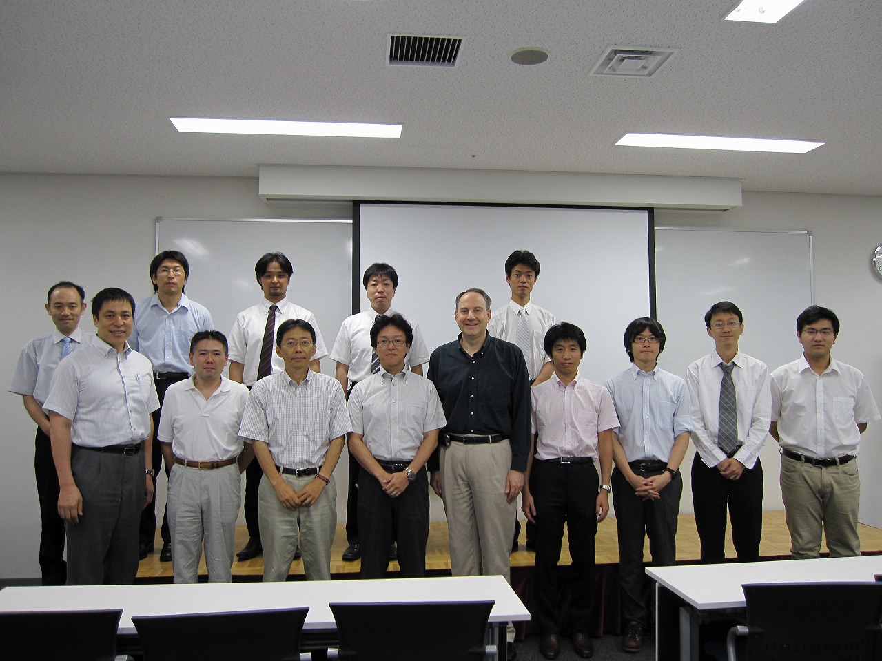
集合写真