日時
会場
所在地:大阪市北区梅田3-4-5 毎日インテシオ3F
Access Map
主催
共催
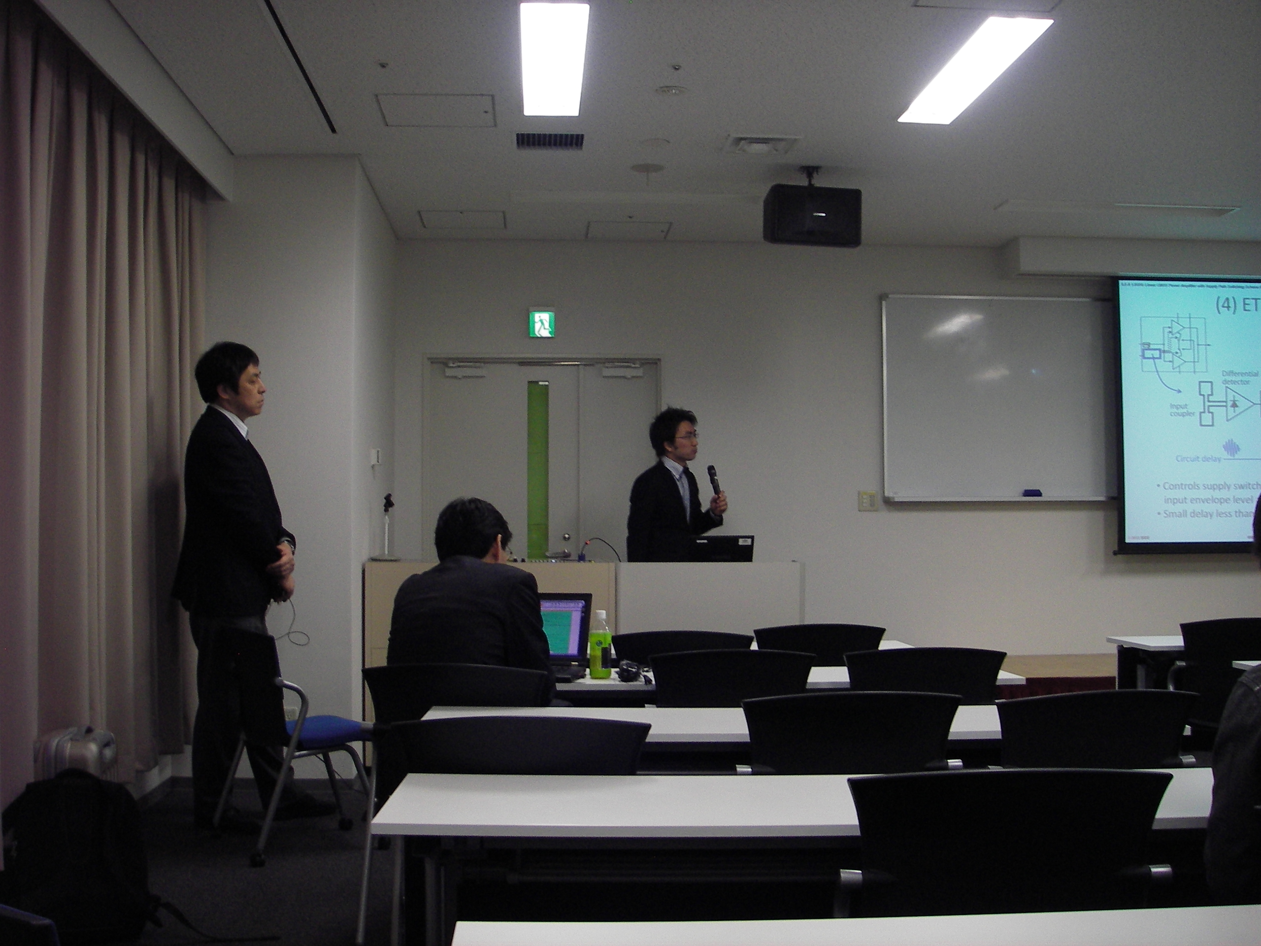
講演
Prof. Makoto Ikeda, University of Tokyo,
ISSCC Far-East Regional Committee Chair
"A 1.8GHz Linear CMOS Power Amplifier with Supply-Path Switching Scheme for WCDMA/LTE Applications"
K. Onizuka, Toshiba
The paper describes a 3.3V linear power amplifier in 65nm CMOS that achieves 27.2dBm output power at 1.8GHz. This PA incorporates a new supply-path switching scheme capable of envelope tracking that improves PAE in the power back-off mode.
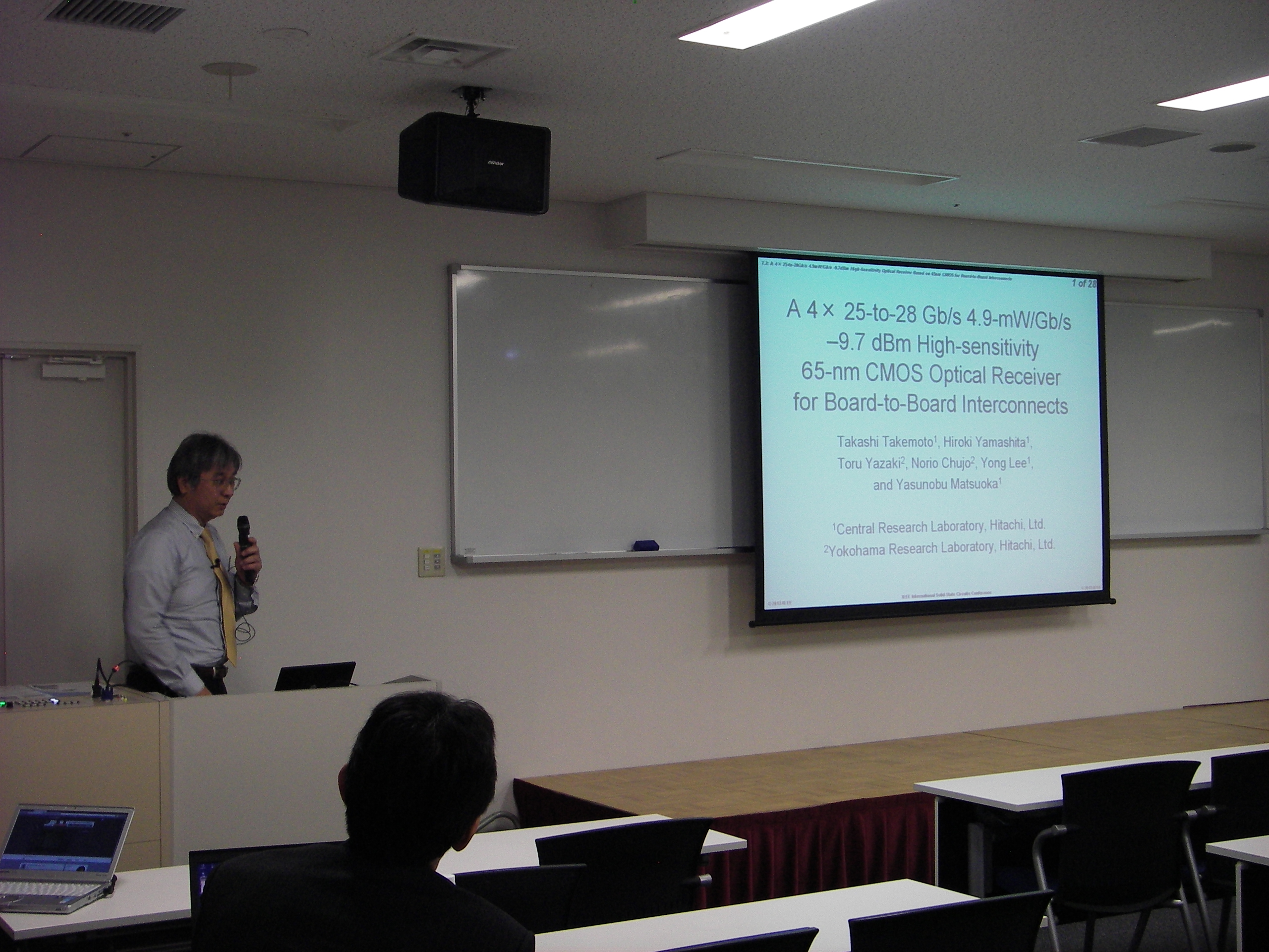
"A 4×25Gb-28Gb/s 4.9mW/Gb/s -9.7dBm High-Sensitivity Optical Receiver based on 65nm CMOS for Board-to-Board Interconnects"
H. Yamashita, Hitachi
The paper demonstrates a 4-channel 25-to-28Gb/s CMOS optical receiver for board-to-board interconnects. The RX incorporates a novel TIA operating at 25Gb/s that achieves the highest sensitivity (-9.7dBm) at the widest eye-opening (65%) reported to date.
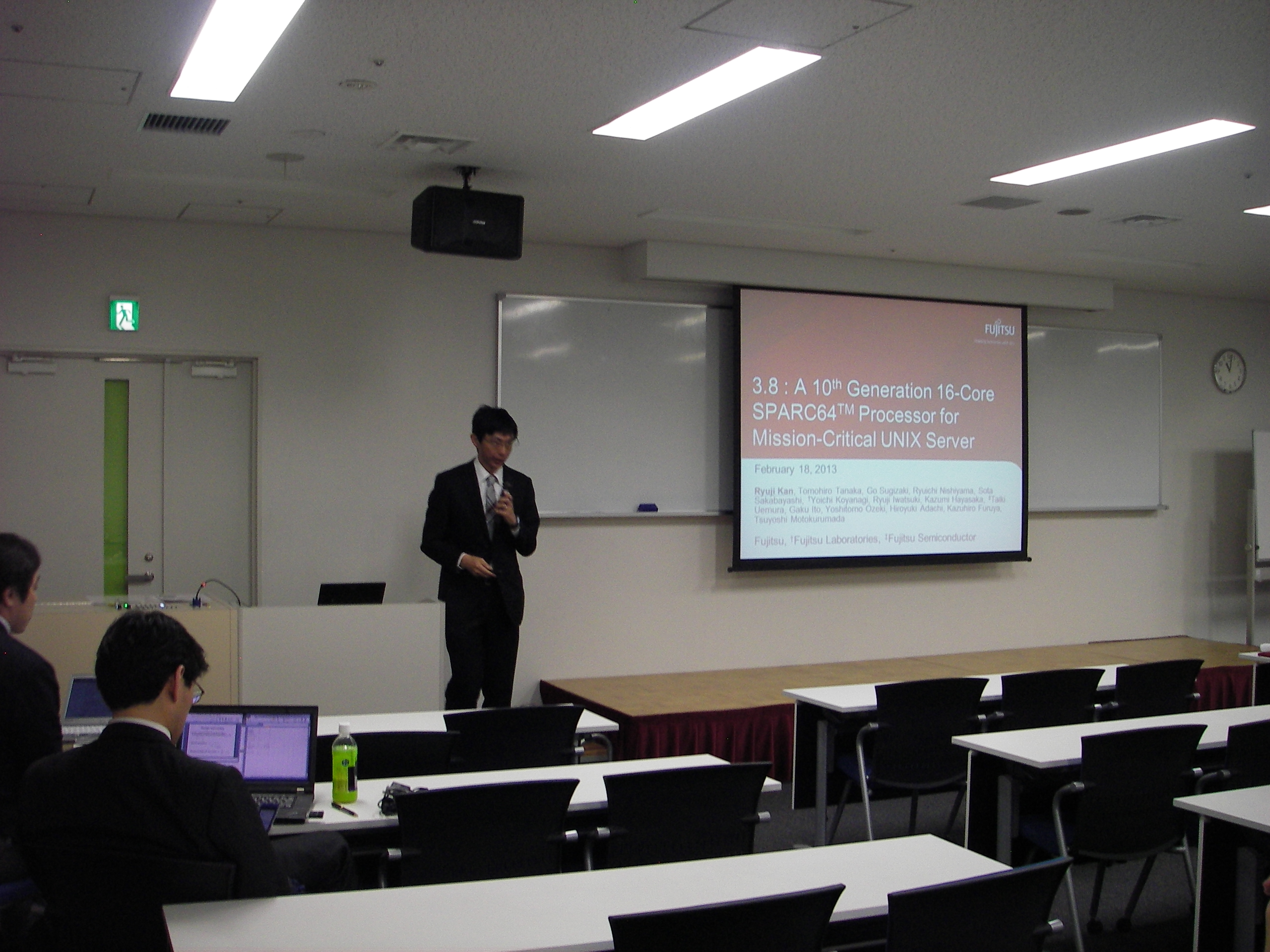
"The 10th Generation 16-Core SPARC64 Processor for Mission-Critical UNIX Server"
R. Kan, Fujitsu
The paper presents a next-generation SPARC64-X processor that runs at 3.0GHz and contains 16 cores with 24MB shared L2 cache and interfaces for system, DDR3, as well as PCIe. Fabricated in 28nm CMOS technology with 13 metal layers on a 588mm2 die, the 3B transistor processor employs newly developed register files and 14.5GB/s SerDes for mission-critical server applications.
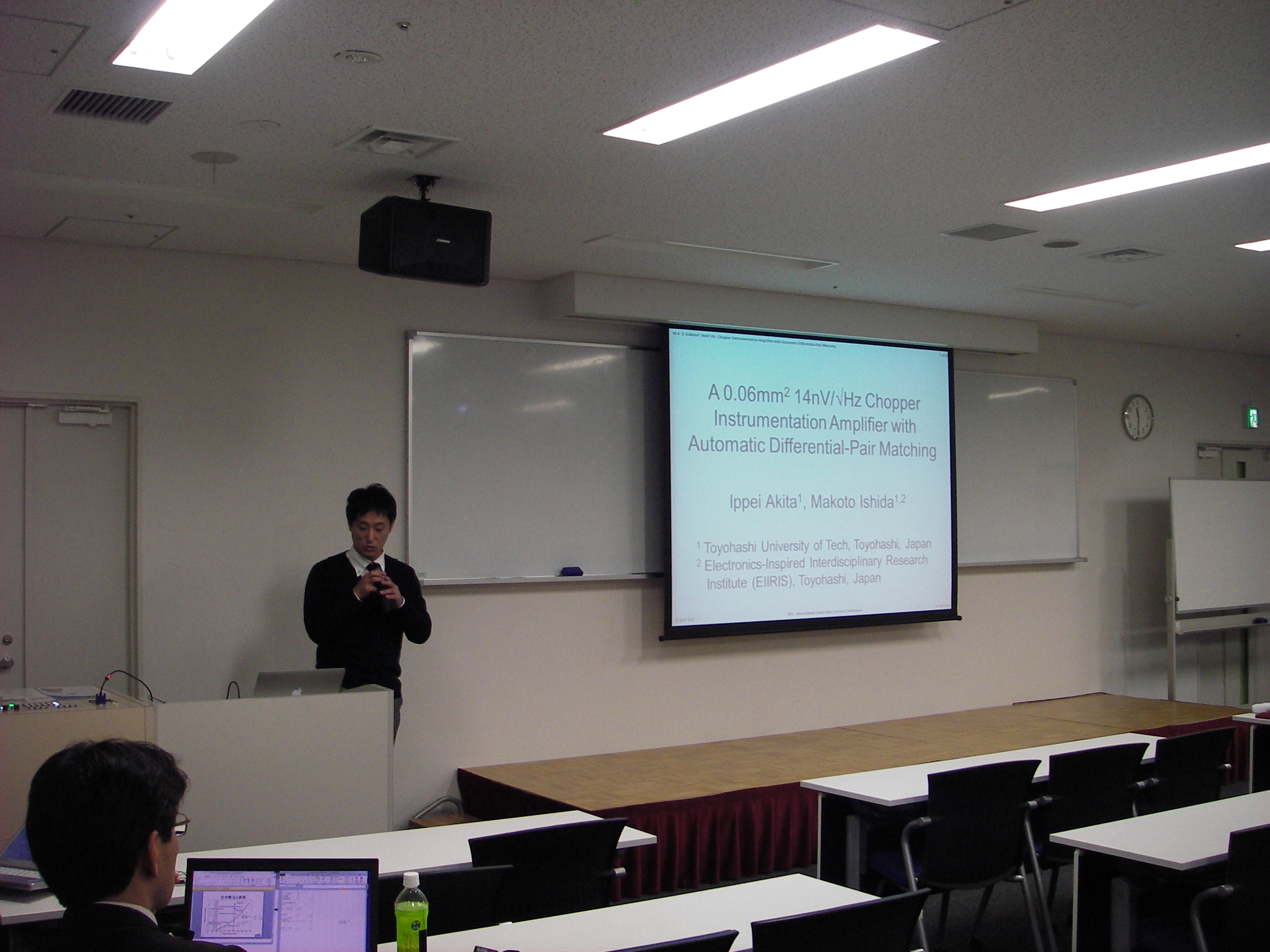
"A 0.06mm2 14nV/√Hz Chopper Instrumentation Amplifier with Automatic Differential-Pair Matching"
I. Akita, Toyohashi University of Technology
The paper presents a 0.06mm2 current-feedback instrumentation amplifier with 32MHz GBW in a standard 0.18μm CMOS. The amplifier uses the chopper-stabilized technique and a novel digital calibration for ripple suppression. The fabricated chip achieves less than 3.5μV offset voltage, 13.5nV/√Hz input referred noise and 194μA current consumption.

"Adaptive Cancellation of Gain and Nonlinearity Errors in Pipelined ADCs"
Y. Miyahara, Asahi Kasei Microdevices
The paper describes an auxiliary amplifier stage to provide nonlinear correction and noise cancellation to achieve 73.3dB SNDR in a 14b pipelined ADC running at 60MS/s. The chip is implemented in 0.18μm CMOS and consumes 68mW from a 1.6V supply.
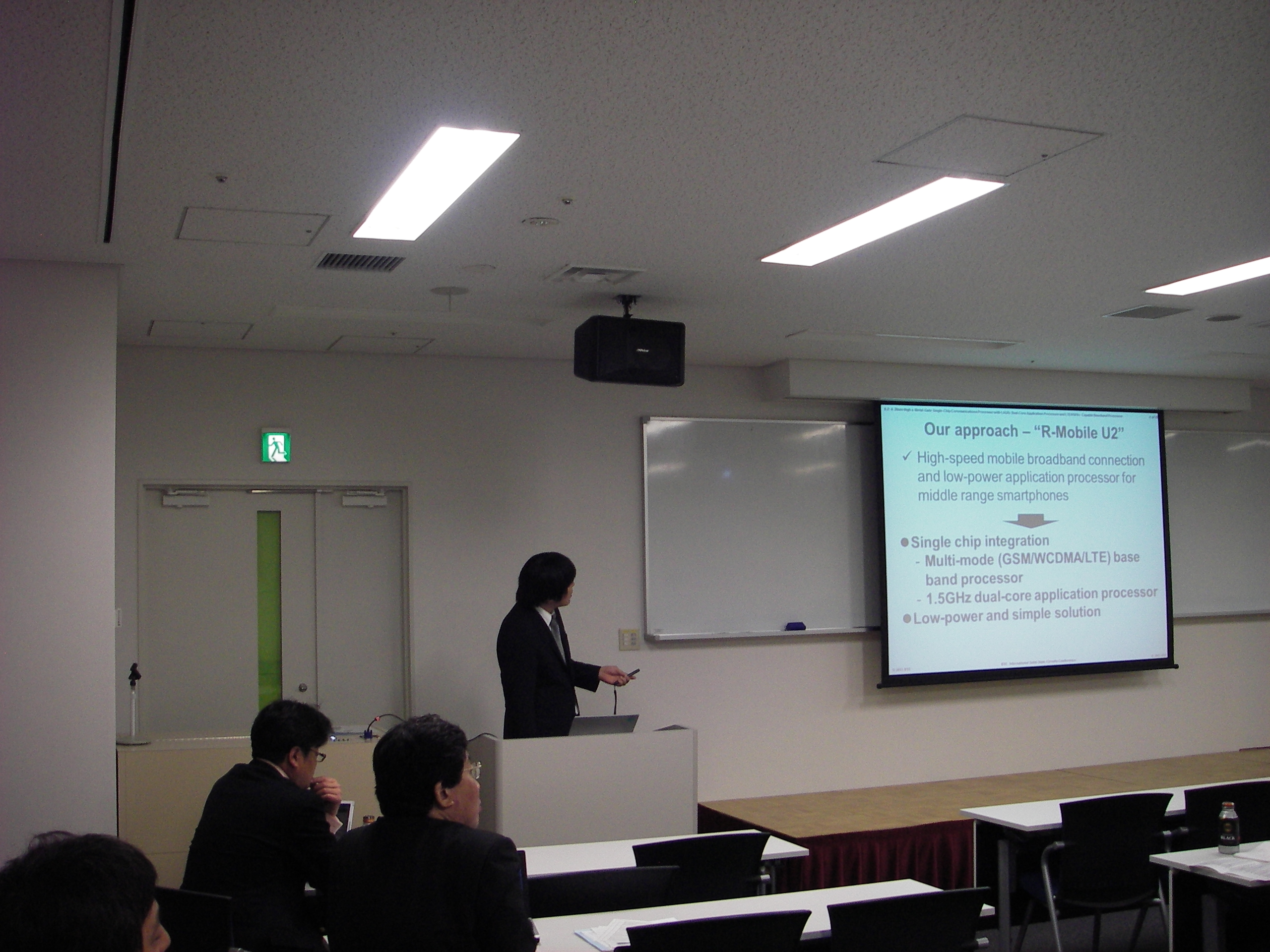
"A 28nm High-k Metal-Gate Single-Chip Communications Processor with 1.5GHz Dual-Core Application Processor and LTE/HSPA+-Capable Baseband Processor"
M. Fujigaya, Renesas Mobile
The paper presents a 28nm high-κ metal-gate low-leakage CMOS bulk process implementation of a single-chip application processor with a dual-core 1.5GHz CPU integrated with a LTE/HSPA+ multimode-baseband modem processor, 2D/3D graphics accelerators, a power management unit and a low-leakage standby mode SRAM design.
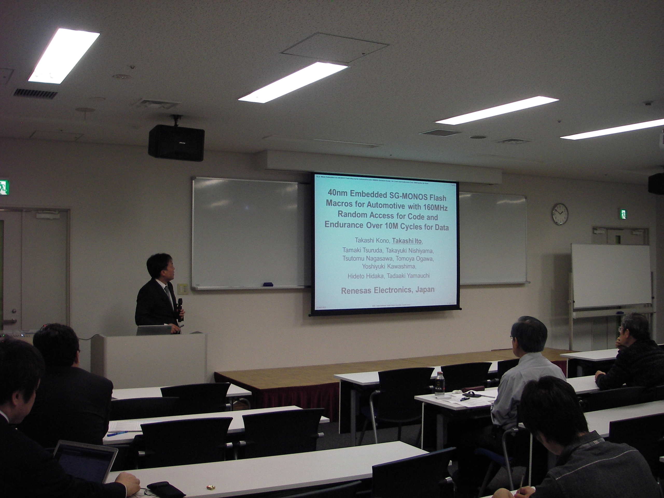
"40nm Embedded SG-MONOS Flash Macros for Automotive with 160MHz Random Access for Code and Endurance Over 10M Cycles for Data"
T. Ito, Renesas Electronics
The paper presents the first-ever 40nm embedded SG-MONOS Flash macros for automotive applications. A SG-MONOS cell, a split-gate memory cell with charge-trapping storage, and three circuit techniques realize random-read access to the code macros at 5.1GB/s. The memory is reliable even at a junction temperature of 170°C
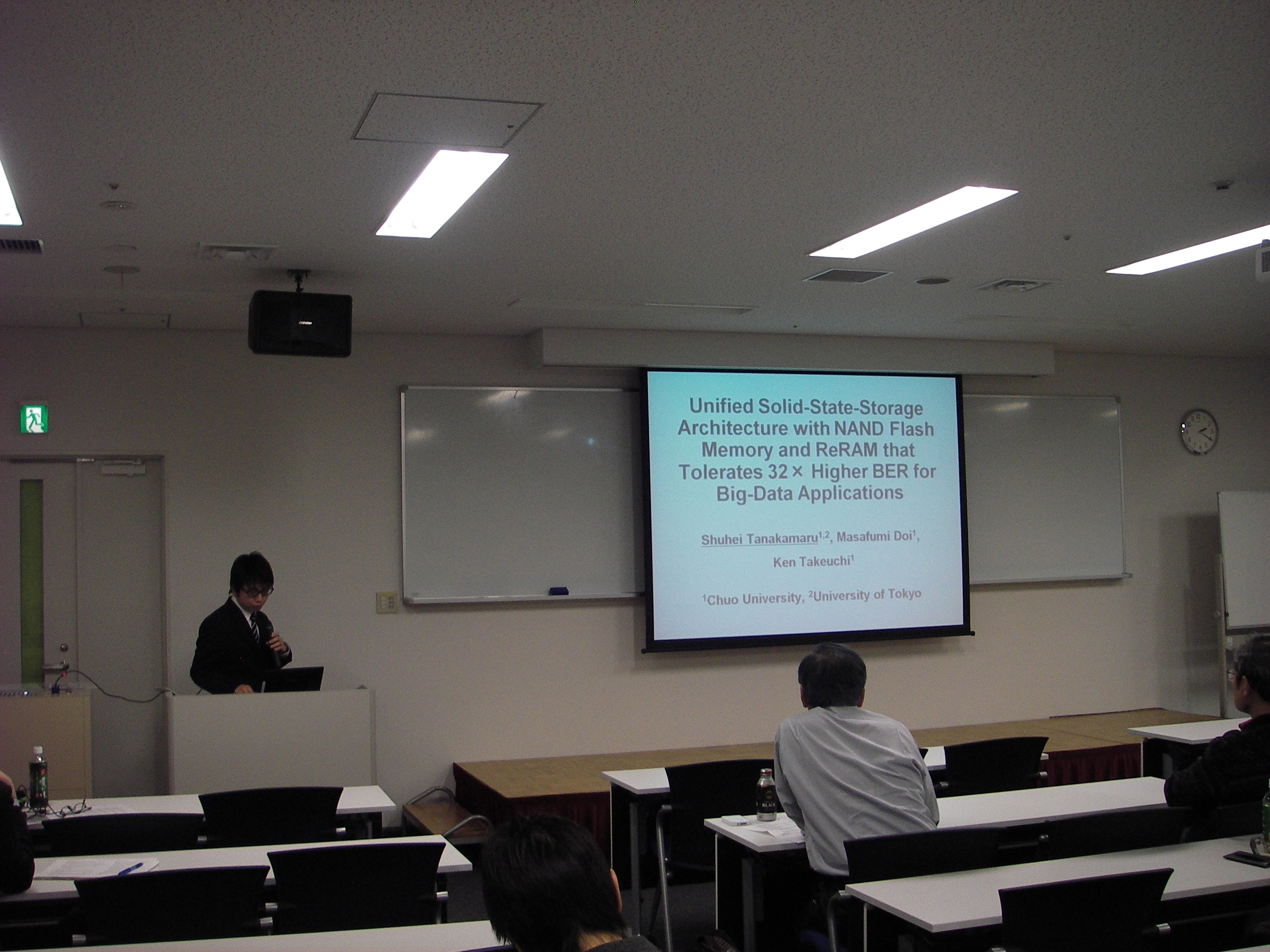
"Unified Solid-State-Storage Architecture with NAND Flash Memory and ReRAM that Tolerates 32× Higher BER for Big-Data Applications"
S. Tanakamaru, Chuo University
The paper presents a solid-state storage architecture that merges NAND Flash memory and ReRAM targeted at big-data applications. The system tolerates a 32× higher BER from the NAND cells by using techniques of reverse-mirroring, error-reduction synthesis, page-RAID, and error-masking.
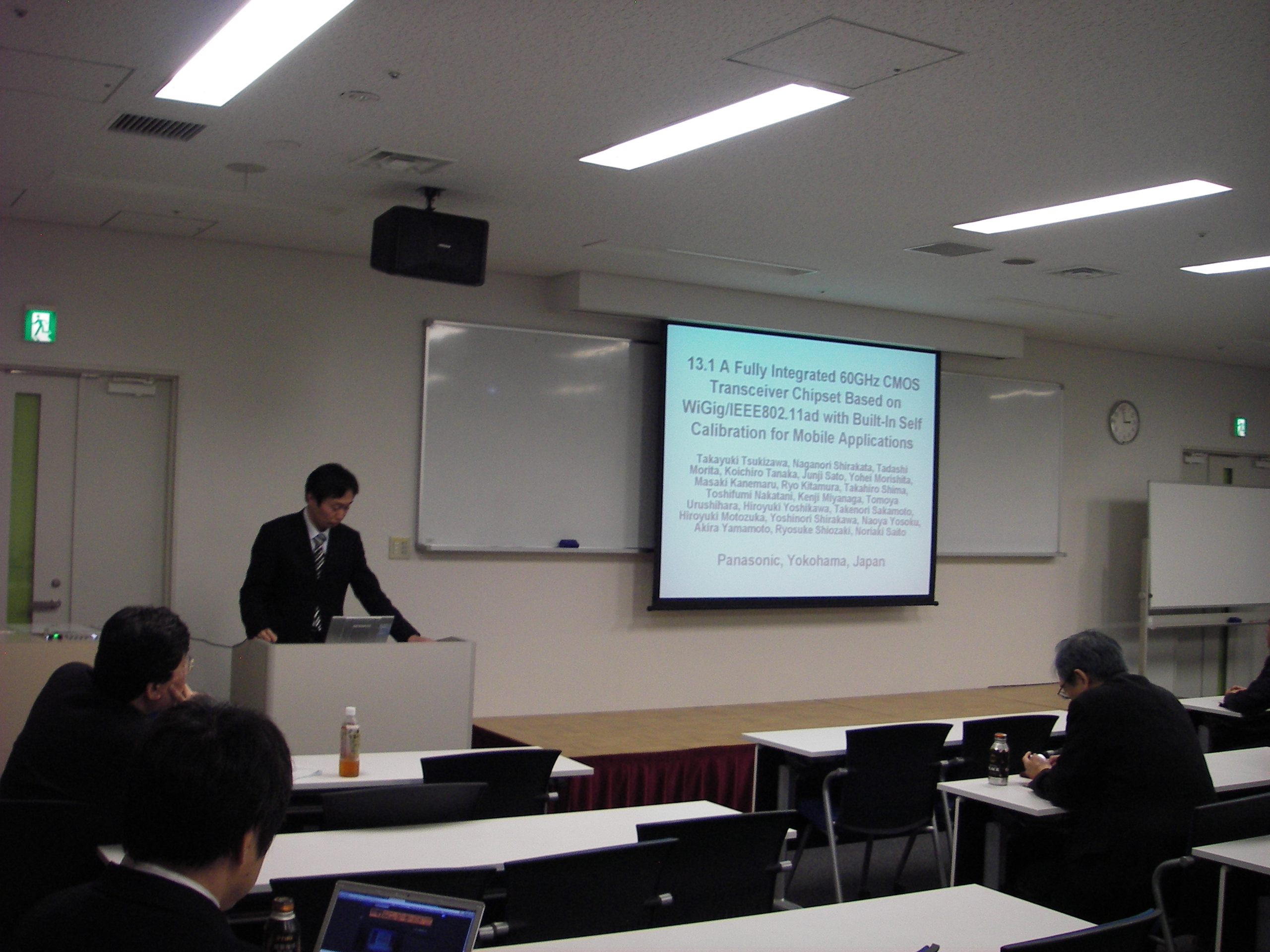
"A Fully Integrated 60GHz CMOS Transceiver Chipset Based on WiGig/IEEE802.11ad with Built-In Self Calibration for Mobile Applications"
T. Tsukizawa, Panasonic
The paper presents the first 60GHz transceiver chipset for WiGig/IEEE802.11ad. The radio achieves 1.8Gb/s MAC throughput while consuming 788mW (TX) and 984mW (RX), and incorporates both mm-Wave front-end and full digital backend in 90nm and 40nm CMOS respectively.
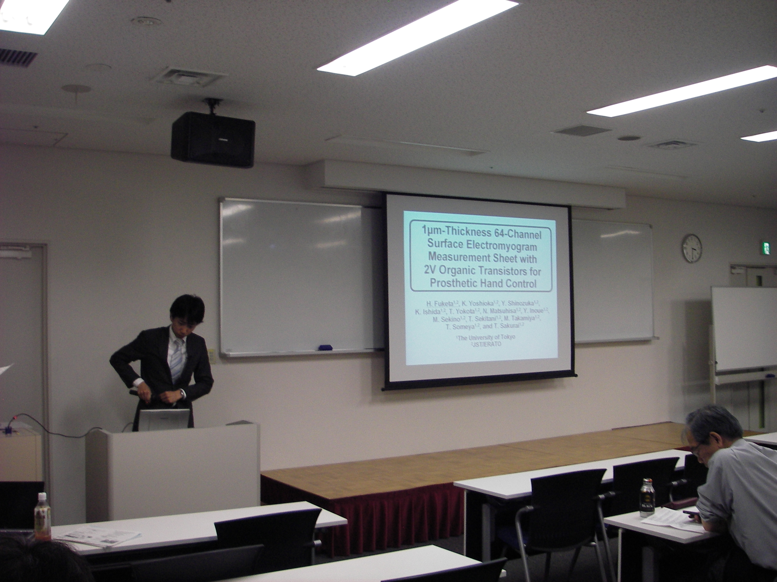
"1μm Thickness 64-Channel Surface Electromyogram Measurement Sheet with 2V Organic Transistors for Prosthetic Hand Control"
H. Fuketa, University of Tokyo
The paper presents a 18cm2 64-channel surface electromyogram measurement sheet implemented with 2V organic transistors for prosthetic hand control. A 4-fold increase in electrode density is achieved using a distributed and shared amplifier architecture while a post-fabrication select-and-connect method reduces transistor mismatch and power consumption.
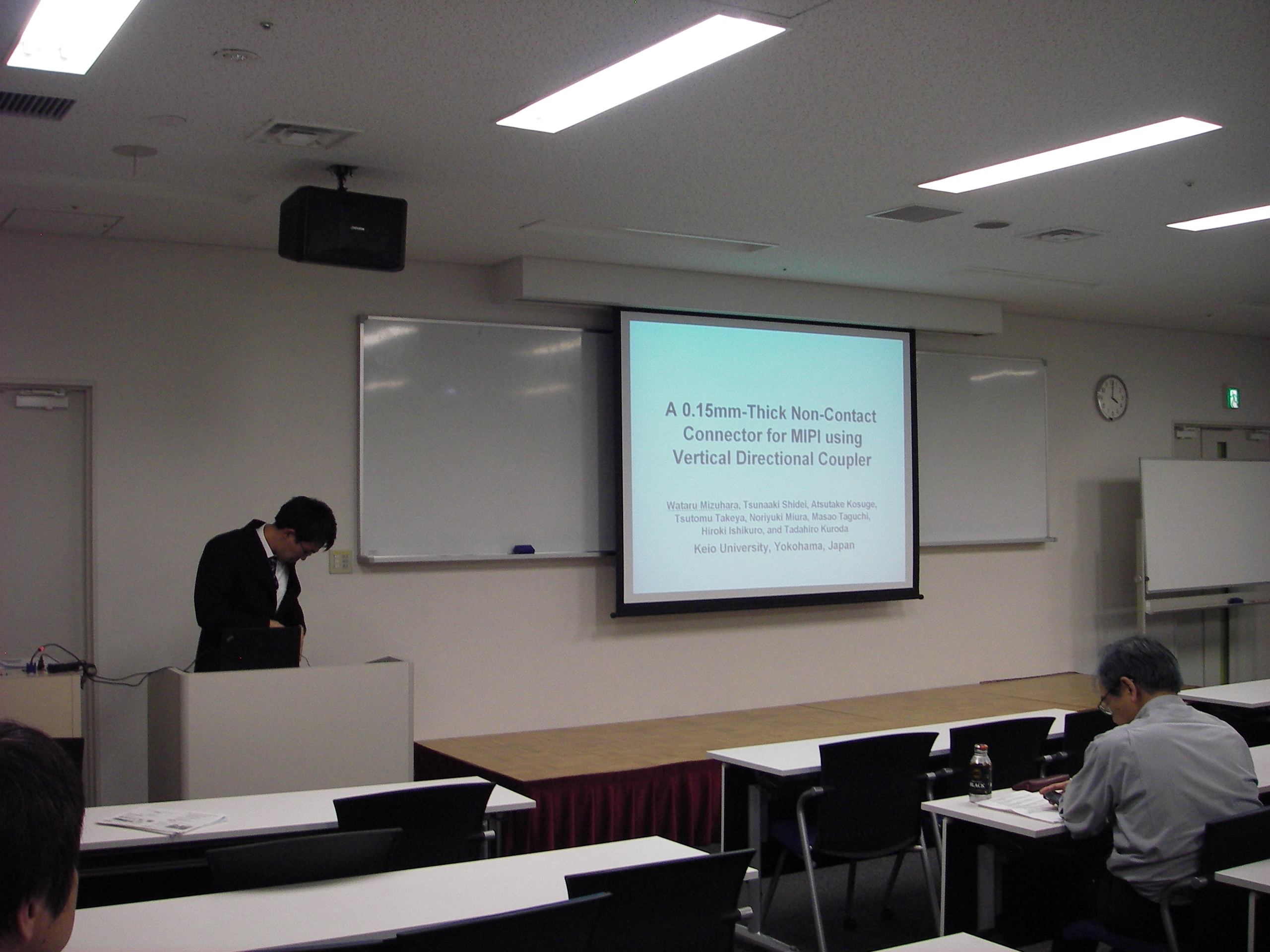
"A 0.15mm-Thick Non-Contact Connector for MIPI using Vertical Directional Coupler"
W. Mizuhara, Keio University
The paper presents a 0.15mm-thick non-contact connector for Mobile Industry Processor Interface (MIPI) applications. A fully balanced pulse transmitter fabricated in 90nm CMOS technology consumes 1.5pJ/b and significantly suppresses EMI, allowing simultaneous two-channel communications.
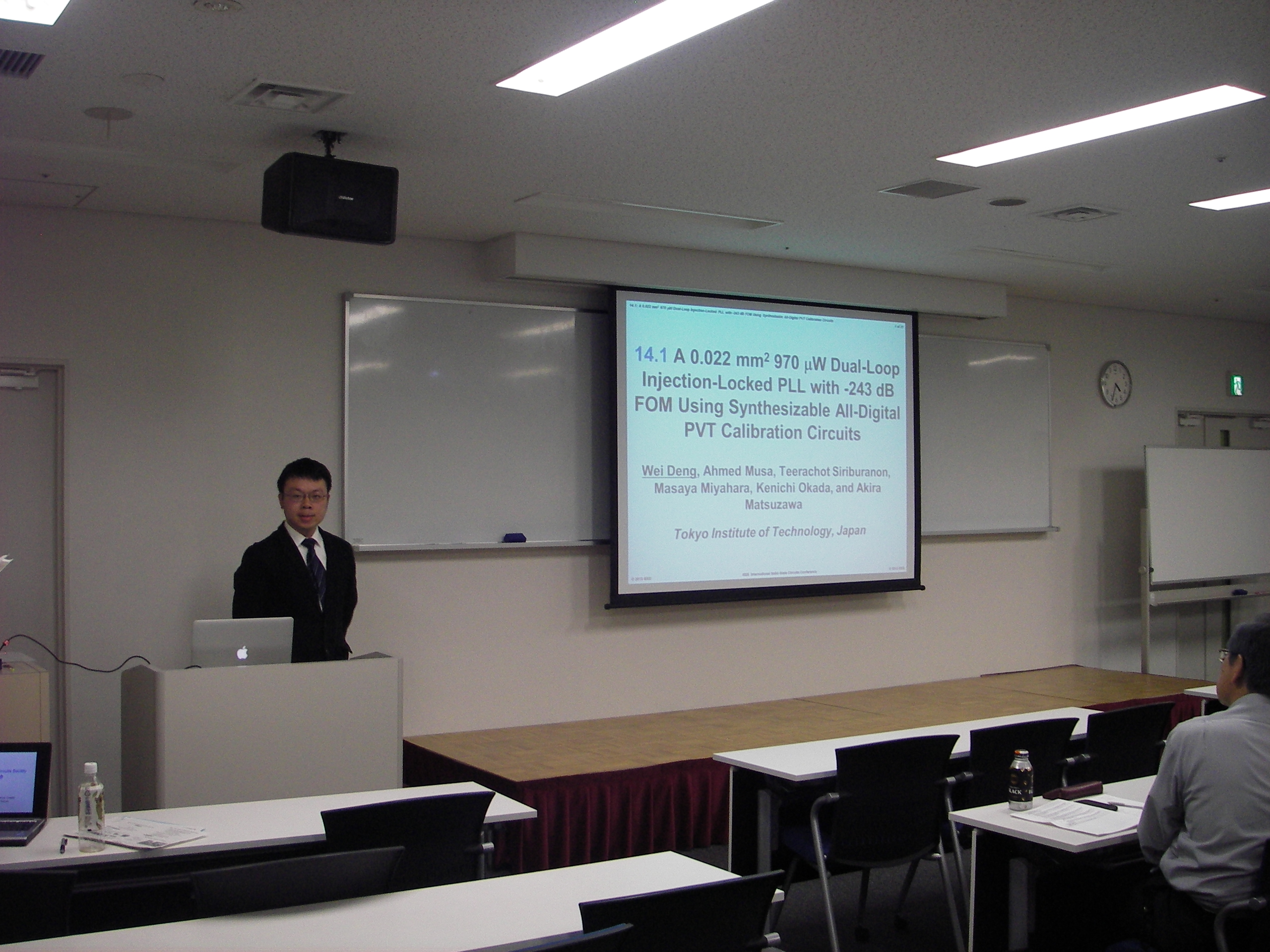
"A 0.022mm2 970μW Dual-loop Injection-Locked PLL with -243 dB FOM Using Synthesizable All-Digital PVT Calibration Circuits"
W. Deng, Tokyo Institute of Technology
The paper presents a 0.022mm2 970mW dual-loop injection-locked PLL implemented in 65nm CMOS and using all-digital PVT-calibration circuits. The small area is achieved using a TDC-less digital FLL with injection locking. The PLL uses both a main loop and a replica loop for PVT tracking resulting in 0.7psRMS jitter.
参加者
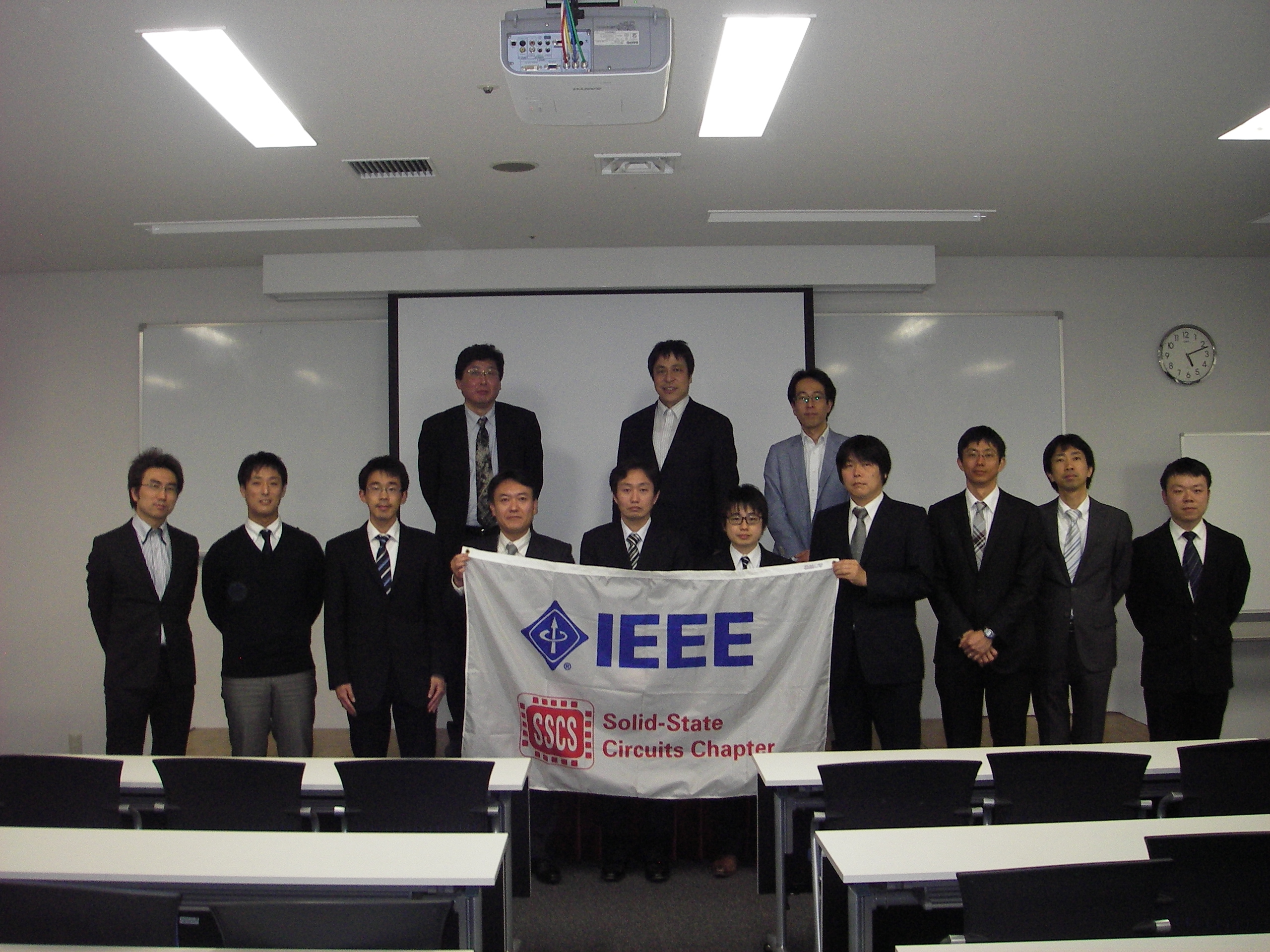
講演者と役員