日時
会場
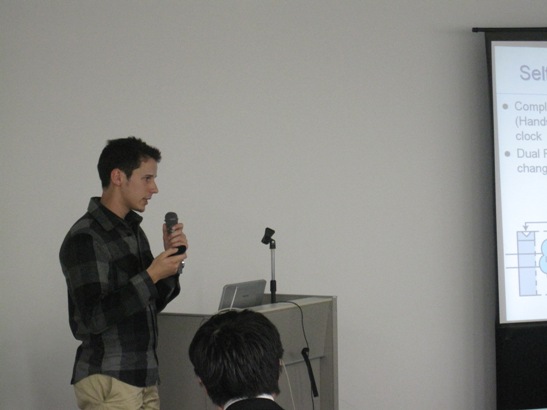
4-5 "A 65nm 2.97GHz self synchronous FPGA with 42% power bounce tolerance"
Benjamin Devlin, University of Tokyo
The performance and robustness to PVT variations has been measured of an improved Self Synchronous FPGA (SSFPGA) designed in 65nm CMOS which achieves 2.97GHz throughput at 1.2V. The proposed SSFPGA employs a 38x38 array of 4-input,3-stage Self Synchronous Configurable Logic Blocks, with the introduction of a new dual tree-divider 4 input LUT to achieve a 4.5x throughput improvement over the previous model [2], [3]. Correct operation is measured with 500mVp-p, 1.12GHz externally introduced power supply noise at 1.2V power supply, equivalent to 42% power supply bounce. Sensitivity against power supply noise frequency has been measured, and showed a strong correlation with the average operating frequency. Correct operation for 10 chips that show 16% performance variation, with VDD change from 728mV to 1.6V, and temperature change from 0 to 80 ℃, without altering any input parameters such as clock frequency. Results show the SSFPGA can adapt and is inherently robust to these variations with a internal throughput measured ranging from 300MHz to 4.07GHz, while maintaining correct operation.
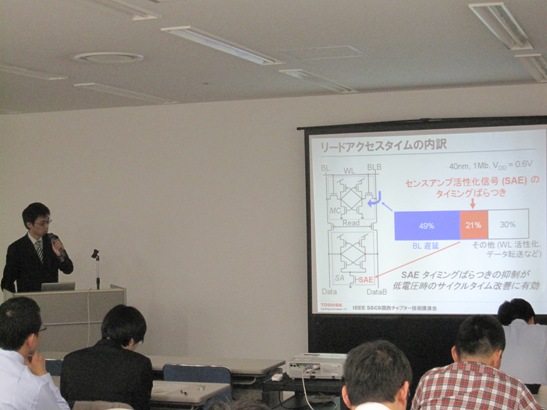
15-1 "A digitized replica bitline delay technique for random-variation tolerant timing generation of SRAM sense amplifiers"
Yusuke Niki, Toshiba Corporation
A digitized replica bitline delay technique has been proposed for random-variation-tolerant timing generation of SRAM sense amplifiers. The sense timing variation attributable to the random variation of transistor threshold voltage is reduced by sufficient count of multiple replica cells, and replica bitline delay is digitized and multiplied for adjusting it to the target sense timing. The variation of the generated timing was 34% smaller than that with a conventional technique and cycle time was reduced by 16% at the supply voltage of 0.6V in 40nm CMOS technology with this scheme.
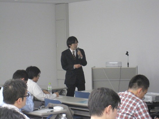
1-2 "A 28nm Dual-port SRAM macro with screening circuitry against write-read disturb failure issues"
Yuichiro Ishii, Renesas Electronics Corporation
We propose a circuit technique for an 8T dual-port (DP) SRAM in order to screen degraded minimum operating voltage (Vmin) due to the write/read disturb issue. This circuitry allows us to generate the write/read disturb condition without relying on the conventional costly asynchronous operation. We designed and fabricated a 512-kb DP-SRAM macro using 28-nm low-power CMOS technology, and confirmed assured screening of failures in the write/read disturb operations.

1-1 "Asymmetric cross-coupled sense amplifier for small0sized 0.5V Gigabit DRAM arrays"
Akira Kotabe, Hitachi Limited
A new sense amplifier (SA) and relevant circuits were proposed for low-power, high-speed, and small-sized 0.5-V gigabit DRAM arrays. The SA, consisting of a low-VT NMOS preamplifier and a cross-coupled high-VT PMOS latch, achieved 46% area reduction compared to our previously proposed SA with a low-VT CMOS preamplifier. Separation of the SA and a data-line pair, and overdrive of the latch achieved a restoring time of 13.4 ns and a sensing time of 6 ns. An adaptive leakage control of the preamplifier reduced the leakage current of the SA to 2% of that without the control.
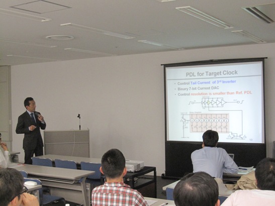
8-3 "A circuit for on chip skew adjustment with jitter and setup time measurement"
Masahiro Sasaki, University of Tokyo
This paper reports a circuit for on-chip skew adjustment with jitter and setup time measurement. A test chip has been fabricated in a 65-nm CMOS process. It successfully measures the random jitter distribution and the relative setup time. This circuit becomes necessary in SoCs because direct measurement cannot be performed by external equipment. Setup time of a D-FF is measured by sweeping over the range of an adjustable input delay line. Its jitter is represented by a Cumulative Distribution Function which is measured by sampling the setup time repeatedly. The skew can be adjusted based on the setup time and jitter determined by our method. Furthermore, this method can be extended for almost any number of Target/Reference Programmable Delay Lines. This system enables designers to adjust skew between the distributed clock paths as well as to measure sub-picosecond level jitter and setup time of D-FFs beyond 10-GHz.
3-1 "A 30Gb/S/Link 2.2Tb/S/mm^2 inductively-coupled injection locking CDR"
Yasuhiro Take, Keio University
This paper presents a 30Gb/s/link 2.2Tb/s/mm2 inductive-coupling link for a high-speed DRAM interface. The data rate per layout area is the highest among DRAM interfaces reported up to now. The proposed interface employs a high-speed injection-locking CDR technique that utilizes the derivative property of inductive coupling. Compared to conventional injection-locking CDR based on an XOR edge detector, our technique doubles the operation speed and increases the data rate to 30Gb/s/link. As a result, the data rate per layout area is increased to 2.2Tb/s/mm2, which is 2X that of the state-of-the-art inductive-coupling link, and 22X that of the state-of-the-art wired link.
7-2 "A 58-63.6GHz Quadrature PLL frequency synthesizer in 65nm CMOS"
Ahmed Musa, Tokyo Institute of Technology
This paper proposes a 60GHz quadrature PLL frequency synthesizer that has a tuning range capable of covering the whole band specified by the IEEE802.15.3c with exceptional phase noise. The synthesizer is constructed using a 20GHz PLL that is coupled with a frequency tripler to generate the 60GHz signal. The 20GHz PLL generates a signal with a phase noise as low as -106dBc/Hz using tail feedback to improve the phase noise. The proposed 60GHz ILO uses a combination of parallel and tail injection to enhance the locking range by reducing the Injection Locked Oscillator (ILO) current at the moment of injection. Both the 20GHz PLL and the ILO were fabricated using a 65nm CMOS process and measurement results show a phase noise of -96dBc/Hz at 60GHz while consuming 77.5mW from a 1.2V supply. To to author’s knowledge this phase noise is about 20dB better then recently reported QPLL and about 10dB compared to di erential PLL operating at similar frequency.

11-1 "A 120GHz transmitter and receiver chipset with 9Gbps data rate using 65nm CMOS technology"
Ryuichi Fujimoto, STARC
The design and measured results of a 120-GHz transmitter and receiver chipset are described in this paper. A simple amplitude shift keying (ASK) is adopted for this chipset. The proposed transmitter and receiver are fabricated using 65nm CMOS technology. The current consumptions are 19.2 mA for the transmitter and 48.2 mA for the receiver. A 9-Gbps PRBS is successfully transferred from the transmitter to the receiver with the bit error rate less than 10-9.
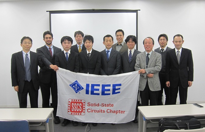
参加者
集合写真